没有合适的资源?快使用搜索试试~ 我知道了~
LT1373-芯片资料介绍.pdf
1.该资源内容由用户上传,如若侵权请联系客服进行举报
2.虚拟产品一经售出概不退款(资源遇到问题,请及时私信上传者)
版权申诉
0 下载量 137 浏览量
2022-07-04
09:02:50
上传
评论
收藏 272KB PDF 举报
温馨提示
试读
12页
LT1373-芯片资料介绍.pdf
资源推荐
资源详情
资源评论
1
LT1373
250kHz Low Supply Current
High Efficiency
1.5A Switching Regulator
■
Boost Regulators
■
CCFL Backlight Driver
■
Laptop Computer Supplies
■
Multiple Output Flyback Supplies
■
Inverting Supplies
APPLICATIONS
U
The LT
®
1373 is a low supply current high frequency
current mode switching regulator. It can be operated in all
standard switching configurations including boost, buck,
flyback, forward, inverting and “Cuk.” A 1.5A high effi-
ciency switch is included on the die, along with all oscilla-
tor, control, and protection circuitry. All functions of the
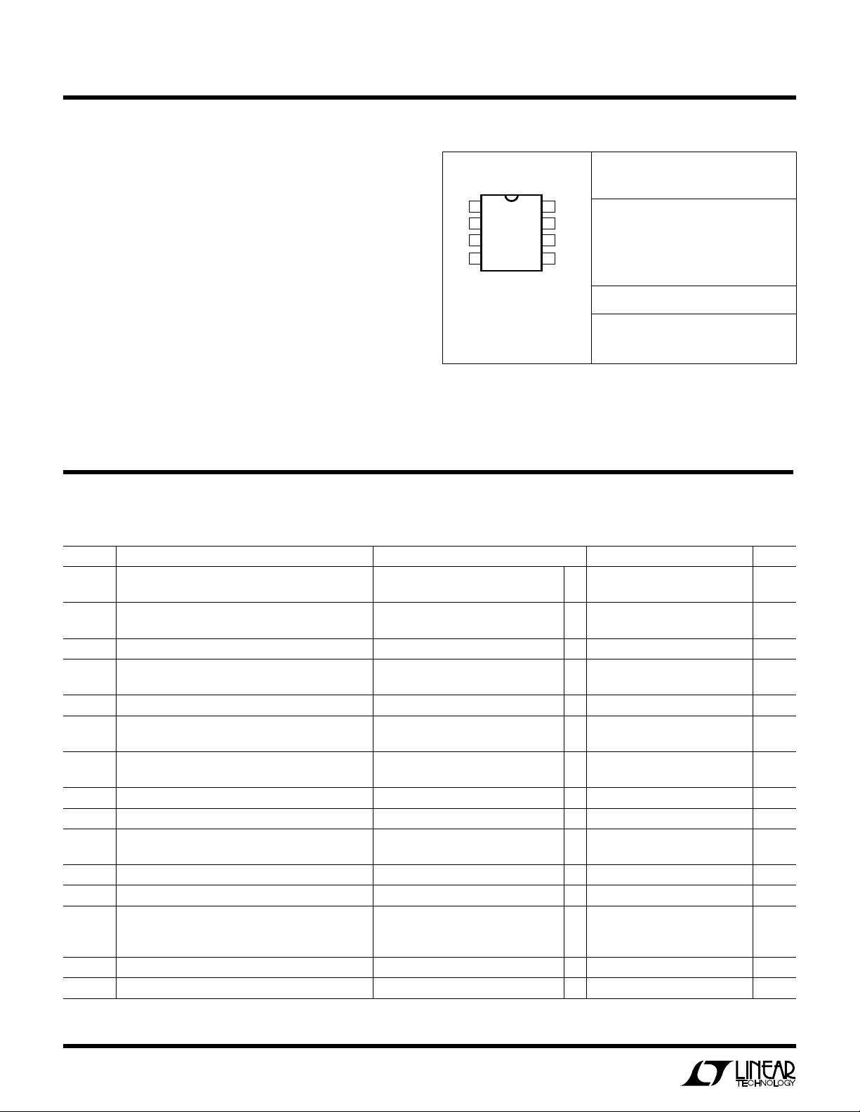
LT1373 are integrated into 8-pin SO/PDIP packages.
Compared to the 500kHz LT1372, which draws 4mA of
quiescent current, the LT1373 switches at 250kHz, typi-
cally consumes only 1mA and has higher efficiency. High
frequency switching allows for small inductors to be used.
All surface mount components consume less than 0.6
square inch of board space.
New design techniques increase flexibility and maintain
ease of use. Switching is easily synchronized to an exter-
nal logic level source. A logic low on the shutdown pin
reduces supply current to 12µA. Unique error amplifier
circuitry can regulate positive or negative output voltage
while maintaining simple frequency compensation tech-
niques. Nonlinear error amplifier transconductance re-
duces output overshoot on start-up or overload recovery.
Oscillator frequency shifting protects external compo-
nents during overload conditions.
DESCRIPTION
U
■
1mA I
Q
at 250kHz
■
Uses Small Inductors: 15µH
■
All Surface Mount Components
■
Only 0.6 Square Inch of Board Space
■
Low Minimum Supply Voltage: 2.7V
■
Constant Frequency Current Mode
■
Current Limited Power Switch: 1.5A
■
Regulates Positive or Negative Outputs
■
Shutdown Supply Current: 12µA Typ
■
Easy External Synchronization
■
8-Pin SO or PDIP Packages
FEATURES
, LTC and LT are registered trademarks of Linear Technology Corporation.
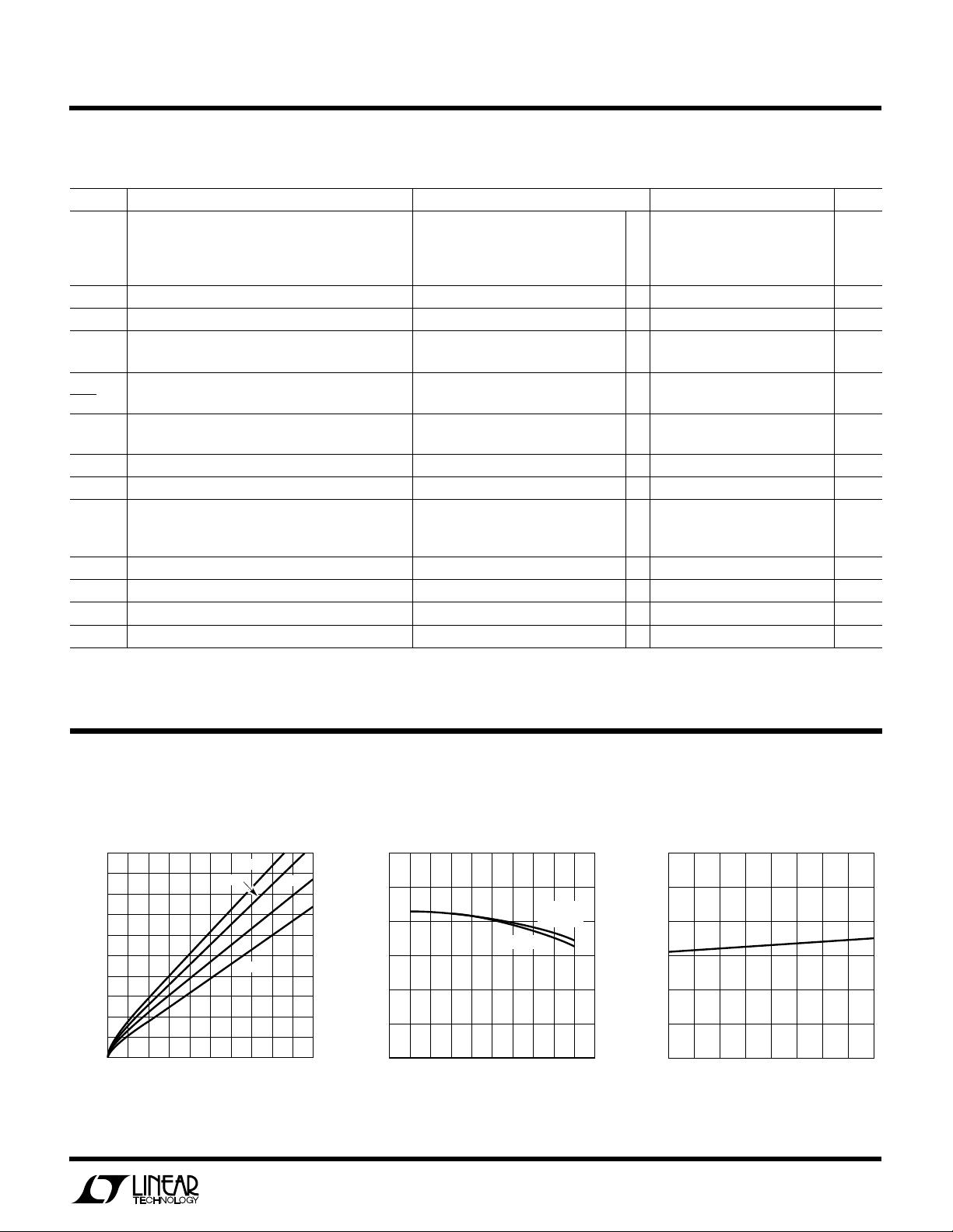
OUTPUT CURRENT (mA)
1
70
EFFICIENCY (%)
80
90
10 100 1000
LT1373 • TA02
60
50
100
V
IN
= 5V
f = 250kHz
TYPICAL APPLICATION
U
LT1373
V
IN
V
C
5V
1
2
8
5
4
6, 7
SUMIDA CD75-220KC (22µH) OR
COILCRAFT D03316-153 (15µH)
AVX TPSD226M025R0200
GND
FB
LT1373 • TA01
V
SW
S/S
L1*
22µH
C1**
22µF
C4**
22µF
C2
0.01µF
R3
5k
R2
24.9k
1%
R1
215k
1%
*
**
V
OUT
†
12V
†
MAX I
OUT
+
+
D1
MBRS120T3
ON
OFF
L1
15µH
22µH
I
OUT
0.3A
0.35A
5V-to-12V Boost Converter
12V Output Efficiency
2
LT1373
A
U
G
W
A
W
U
W
ARB
S
O
LU
T
EXI T
I
S
WU
U
PACKAGE
/
O
RDER I FOR ATIO
Consult factory for Military grade parts.
Supply Voltage ....................................................... 30V
Switch Voltage
LT1373 ............................................................... 35V
LT1373HV .......................................................... 42V
S/S Pin Voltage....................................................... 30V
Feedback Pin Voltage (Transient, 10ms) .............. ±10V
Feedback Pin Current........................................... 10mA
Negative Feedback Pin Voltage
(Transient, 10ms)............................................. ±10V
Operating Junction Temperature Range
Commercial ........................................ 0°C to 125°C*
Industrial ......................................... –40°C to 125°C
Short Circuit ......................................... 0°C to 150°C
Storage Temperature Range ................ –65°C to 150°C
Lead Temperature (Soldering, 10 sec)................. 300°C
LT1373CN8
LT1373HVCN8
LT1373CS8
LT1373HVCS8
LT1373IN8
LT1373HVIN8
LT1373IS8
LT1373HVIS8
S8 PART MARKING
ORDER PART
NUMBER
1373H
1373HI
1373
1373I
*Units shipped prior to Date Code 9552 are rated at 100°C maximum
operating temperature.
SYMBOL PARAMETER CONDITIONS MIN TYP MAX UNITS
V
REF
Reference Voltage Measured at Feedback Pin 1.230 1.245 1.260 V
V
C
= 0.8V ● 1.225 1.245 1.265 V
I
FB
Feedback Input Current V
FB
= V
REF
50 150 nA
● 275 nA
Reference Voltage Line Regulation 2.7V ≤ V
IN
≤ 25V, V
C
= 0.8V ● 0.01 0.03 %/V
V
NFB
Negative Feedback Reference Voltage Measured at Negative Feedback Pin –2.490 V
Feedback Pin Open, V
C
= 0.8V ● –2.490 V
I
NFB
Negative Feedback Input Current V
NFB
= V
NFR
● –12 –7 –2 µA
Negative Feedback Reference Voltage 2.7V ≤ V
IN
≤ 25V, V
C
= 0.8V ● 0.01 0.05 %/V
Line Regulation
g
m
Error Amplifier Transconductance ∆I
C
= ±5µA 250 375 500 µmho
● 150 600 µmho
Error Amplifier Source Current V
FB
= V
REF
– 150mV, V
C
= 1.5V ● 25 50 90 µA
Error Amplifier Sink Current V
FB
= V
REF
+ 150mV, V
C
= 1.5V ● 850 1500 µA
Error Amplifier Clamp Voltage High Clamp, V
FB
= 1V 1.70 1.95 2.30 V
Low Clamp, V
FB
= 1.5V 0.25 0.40 0.52 V
A
V
Error Amplifier Voltage Gain 250 V/V
V
C
Pin Threshold Duty Cycle = 0% 0.8 1 1.25 V
f Switching Frequency 2.7V ≤ V
IN
≤ 25V 225 250 275 kHz
0°C ≤ T
J
≤ 125°C ● 210 250 290 kHz
–40°C ≤ T
J
≤ 0°C (I Grade) 200 290 kHz
Maximum Switch Duty Cycle ● 90 95 %
Switch Current Limit Blanking Time 340 500 ns
E
LECTR
IC
AL C CHARA TERIST
ICS
V
IN
= 5V, V
C
= 0.6V, V
FB
= V
REF
, V
SW
, S/S and NFB pins open, unless otherwise noted.
1
2
3
4
8
7
6
5
TOP VIEW
V
C
FB
NFB
S/S
V
SW
GND
GND S
V
IN
N8 PACKAGE
8-LEAD PDIP
S8 PACKAGE
8-LEAD PLASTIC SO
T
JMAX
= 125°C, θ
JA
= 100°C/ W (N8)
T
JMAX
= 125°C, θ
JA
= 120°C/ W (S8)
3
LT1373
SYMBOL PARAMETER CONDITIONS MIN TYP MAX UNITS
BV Output Switch Breakdown Voltage LT1373 ● 35 47 V
LT1373HV
0°C ≤ T
J
≤ 125°C ● 42 47 V
–40°C ≤ T
J
≤ 0°C (I Grade) 40 V
V
SAT
Output Switch “On” Resistance I
SW
= 1A ● 0.5 0.85 Ω
I
LIM
Switch Current Limit Duty Cycle = 50% ● 1.5 1.9 2.7 A
Duty Cycle = 80% (Note 1) ● 1.3 1.7 2.5 A
∆I
IN
Supply Current Increase During Switch On-Time 10 20 mA/A
∆I
SW
Control Voltage to Switch Current 2A/V
Transconductance
Minimum Input Voltage ● 2.4 2.7 V
I
Q
Supply Current 2.7V ≤ V
IN
≤ 25V ● 1 1.5 mA
Shutdown Supply Current 2.7V ≤ V
IN
≤ 25V, V
S/S
≤ 0.6V
0°C ≤ T
J
≤ 125°C ● 12 30 µA
–40°C ≤ T
J
≤ 0°C (I Grade) 50 µA
Shutdown Threshold 2.7V ≤ V
IN
≤ 25V ● 0.6 1.3 2 V
Shutdown Delay ● 5 12 100 µs
S/S Pin Input Current 0V ≤ V
S/S
≤ 5V ● –10 15 µA
Synchronization Frequency Range ● 300 360 kHz
E
LECTR
IC
AL C CHARA TERIST
ICS
V
IN
= 5V, V
C
= 0.6V, V
FB
= V
REF
, V
SW
, S/S and NFB pins open, unless otherwise noted.
The ● denotes specifications which apply over the full operating
temperature range.
Note 1: For duty cycles (DC) between 50% and 90%, minimum
guaranteed switch current is given by I
LIM
= 0.667 (2.75 – DC).
TYPICAL PERFORMANCE CHARACTERISTICS
U
W
SWITCH CURRENT (A)
0
SWITCH SATURATION VOLTAGE (V)
0.6
0.8
1.0
1.6
LT1373 • G01
0.4
0.2
0.5
0.7
0.9
0.3
0.1
0
0.4
0.8
1.2
2.0
1.4
0.2
0.6
1.0
1.8
100°C
150°C
25°C
–55°C
Switch Saturation Voltage
vs Switch Current
TEMPERATURE (°C)
–50
1.8
INPUT VOLTAGE (V)
2.0
2.2
2.4
2.6
050
100
150
LT1373 • G03
2.8
3.0
–25 25
75
125
Minimum Input Voltage
vs Temperature
DUTY CYCLE (%)
0
SWITCH CURRENT LIMIT (A)
1.0
2.0
3.0
0.5
1.5
2.5
20 40 60 80
LT1373 • G02
10010
0
30 50 70 90
25°C AND
125°C
–55°C
Switch Current Limit
vs Duty Cycle
剩余11页未读,继续阅读
资源评论
书博教育
- 粉丝: 1
- 资源: 2835
上传资源 快速赚钱
- 我的内容管理 展开
- 我的资源 快来上传第一个资源
- 我的收益 登录查看自己的收益
- 我的积分 登录查看自己的积分
- 我的C币 登录后查看C币余额
- 我的收藏
- 我的下载
- 下载帮助
安全验证
文档复制为VIP权益,开通VIP直接复制
信息提交成功