没有合适的资源?快使用搜索试试~ 我知道了~
MCP6S26-芯片资料介绍.pdf
1.该资源内容由用户上传,如若侵权请联系客服进行举报
2.虚拟产品一经售出概不退款(资源遇到问题,请及时私信上传者)
版权申诉
0 下载量 17 浏览量
2022-07-04
08:37:11
上传
评论
收藏 881KB PDF 举报
温馨提示
试读
43页
MCP6S26-芯片资料介绍.pdf
资源推荐
资源详情
资源评论
2003 Microchip Technology Inc. DS21117A-page 1
M
MCP6S21/2/6/8
Features
• Multiplexed Inputs: 1, 2, 6 or 8 channels
• 8 Gain Selections:
- +1, +2, +4, +5, +8, +10, +16 or +32 V/V
• Serial Peripheral Interface (SPI™)
• Rail-to-Rail Input and Output
• Low Gain Error: ±1% (max)
• Low Offset: ±275 µV (max)
• High Bandwidth: 2 to 12 MHz (typ)
• Low Noise: 10 nV/√Hz @ 10 kHz (typ)
• Low Supply Current: 1.0 mA (typ)
• Single Supply: 2.5V to 5.5V
Typical Applications
• A/D Converter Driver
• Multiplexed Analog Applications
• Data Acquisition
• Industrial Instrumentation
• Test Equipment
• Medical Instrumentation
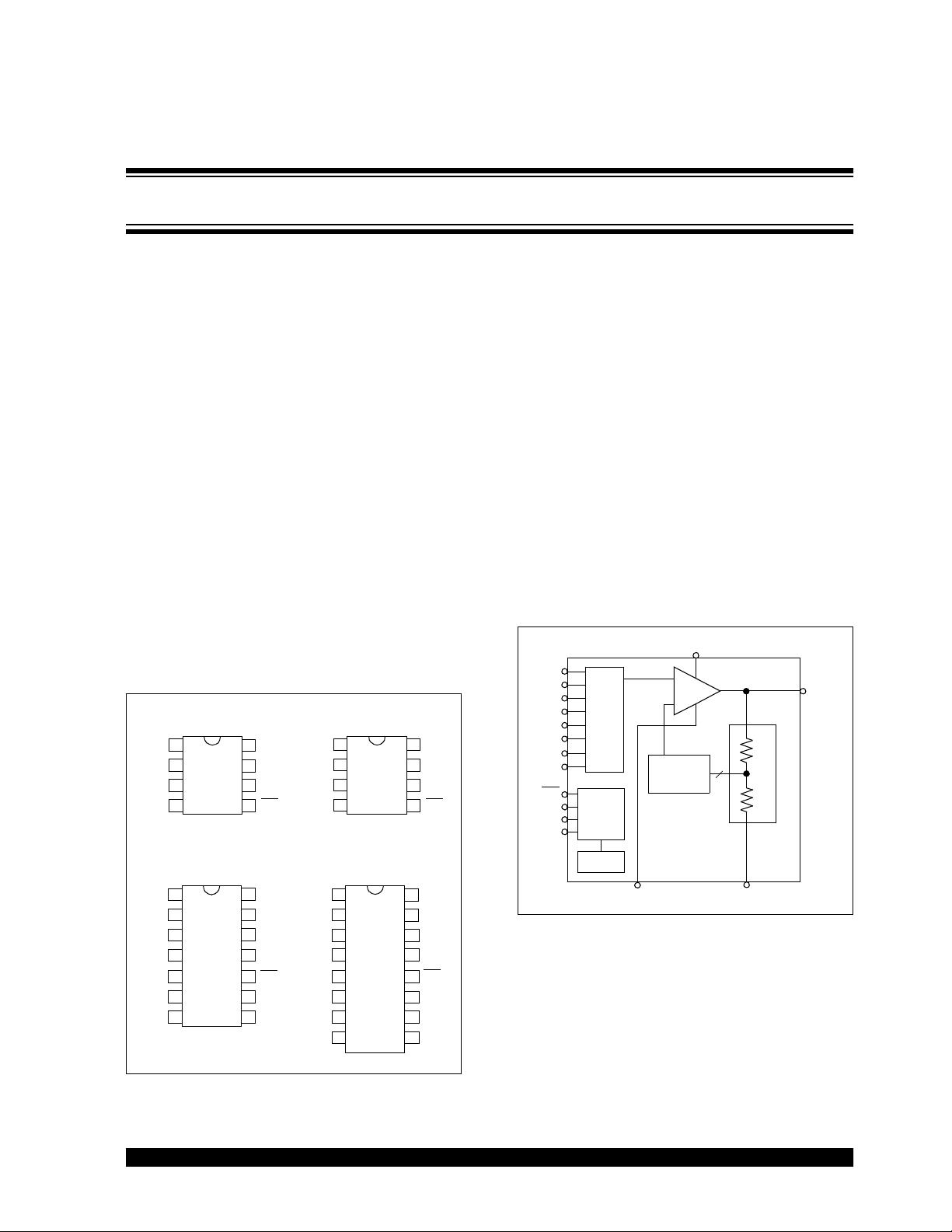
Package Types
Description
The Microchip Technology Inc. MCP6S21/2/6/8 are
analog Programmable Gain Amplifiers (PGA). They
can be configured for gains from +1 V/V to +32 V/V and
the input multiplexer can select one of up to eight chan-
nels through an SPI port. The serial interface can also
put the PGA into shutdown to conserve power. These
PGAs are optimized for high speed, low offset voltage
and single-supply operation with rail-to-rail input and
output capability. These specifications support single
supply applications needing flexible performance or
multiple inputs.
The one channel MCP6S21 and the two channel
MCP6S22 are available in 8-pin PDIP, SOIC and
MSOP packages. The six channel MCP6S26 is avail-
able in 14-pin PDIP, SOIC and TSSOP packages. The
eight channel MCP6S28 is available in 16-pin PDIP
and SOIC packages. All parts are fully specified from
-40°C to +85°C.
Block Diagram
V
REF
CH0
V
SS
SI
SCK
1
2
3
4
8
7
6
5
V
DD
CS
V
OUT
CH1
CH0
CH2
CS
SI
1
2
3
4
14
13
12
11
V
REF
V
SS
V
OUT
5
6
7
10
9
8
CH3
SCK
V
DD
CH5
CH4
CH0
V
OUT
CH1
V
SS
CS
1
2
3
4
16
15
14
13 SI
SCK
5
6
7
12
11
10
CH2
CH4
CH7
V
DD
CH5
8
9
SO
CH6
CH3
SO
CH1
CH0
V
SS
SI
SCK
1
2
3
4
8
7
6
5
V
DD
CS
V
OUT
MCP6S21
PDIP, SOIC, MSOP
MCP6S26
PDIP, SOIC, TSSOP
MCP6S28
PDIP, SOIC
MCP6S22
PDIP, SOIC, MSOP
V
REF
V
OUT
V
REF
V
DD
CS
SI
SO
SCK
CH1
CH0
CH3
CH2
CH5
CH4
CH7
CH6
V
SS
8
R
F
R
G
MUX
SPI™
Logic
POR
Gain
Switches
+
-
Resistor Ladder (R
LAD
)
Single-Ended, Rail-to-Rail I/O, Low Gain PGA
MCP6S21/2/6/8
DS21117A-page 2 2003 Microchip Technology Inc.
1.0 ELECTRICAL
CHARACTERISTICS
Absolute Maximum Ratings †
V
DD
- V
SS
.........................................................................7.0V
All inputs and outputs....................... V
SS
- 0.3V to V
DD
+0.3V
Difference Input voltage ........................................ |V
DD
- V
SS
|
Output Short Circuit Current...................................continuous
Current at Input Pin .............................................................±2mA
Current at Output and Supply Pins ................................ ±30 mA
Storage temperature .....................................-65°C to +150°C
Junction temperature .................................................. +150°C
ESD protection on all pins (HBM;MM).................. ≥ 2 kV; 200V
† Notice: Stresses above those listed under "Maximum
Ratings" may cause permanent damage to the device. This is
a stress rating only and functional operation of the device at
those or any other conditions above those indicated in the
operation listings of this specification is not implied. Exposure
to maximum rating conditions for extended periods may affect
device reliability.
PIN FUNCTION TABLE
Name Function
V
OUT
Analog Output
CH0-CH7 Analog Inputs
V
SS
Negative Power Supply
V
DD
Positive Power Supply
SCK SPI Clock Input
SI SPI Serial Data Input
SO SPI Serial Data Output
CS
SPI Chip Select
V
REF
External Reference Pin
DC CHARACTERISTICS
Electrical Specifications: Unless otherwise indicated, T
A
=+25°C, V
DD
= +2.5V to +5.5V, V
SS
= GND, V
REF
= V
SS
, G = +1 V/V,
Input = CH0 = (0.3V)/G, CH1 to CH7 = 0.3V, R
L
=10kΩ to V
DD
/2, SI and SCK are tied low and CS is tied high.
Parameters Sym Min Typ Max Units Conditions
Amplifier Input
Input Offset Voltage V
OS
-275 — +275 µV G = +1, V
DD
= 4.0V
Input Offset Voltage Drift ∆V
OS
/∆T
A
—±4 —µV/°CT
A
= -40 to +85°C
Power Supply Rejection Ratio PSRR 70 85 — dB G = +1 (Note 1)
Input Bias Current I
B
— ±1 — pA CHx = V
DD
/2
Input Bias Current over
Temperature
I
B
— — 250 pA T
A
= -40 to +85°C,
CHx = V
DD
/2
Input Impedance Z
IN
—10
13
||15 — Ω||pF
Input Voltage Range V
IVR
V
SS
−0.3 — V
DD
+0.3 V
Amplifier Gain
Nominal Gains G — 1 to 32 — V/V +1, +2, +4, +5, +8, +10, +16 or +32
DC Gain Error G = +1 g
E
-0.1 — +0.1 % V
OUT
≈ 0.3V to V
DD
− 0.3V
G ≥ +2 g
E
-1.0 — +1.0 % V
OUT
≈ 0.3V to V
DD
− 0.3V
DC Gain Drift G = +1 ∆G/∆T
A
— ±0.0002 — %/°C T
A
= -40 to +85°C
G ≥ +2 ∆G/∆T
A
— ±0.0004 — %/°C T
A
= -40 to +85°C
Internal Resistance R
LAD
3.4 4.9 6.4 kΩ (Note 1)
Internal Resistance over
Temperature
∆R
LAD
/∆T
A
—+0.028 — %/°C(Note 1)
T
A
= -40 to +85°C
Amplifier Output
DC Output Non-linearity G = +1 V
ONL
— ±0.003 — % of FSR V
OUT
= 0.3V to V
DD
− 0.3V, V
DD
= 5.0V
G ≥ +2 V
ONL
— ±0.001 — % of FSR V
OUT
= 0.3V to V
DD
− 0.3V, V
DD
= 5.0V
Maximum Output Voltage Swing V
OH
, V
OL
V
SS
+20 — V
DD
-100 mV G ≥ +2; 0.5V output overdrive
V
SS
+60 — V
DD
-60 G ≥ +2; 0.5V output overdrive,
V
REF
= V
DD
/2
Short-Circuit Current I
O(SC)
—±30 — mA
Note 1: R
LAD
(R
F
+ R
G
in Figure 4-1) connects V
REF
, V
OUT
and the inverting input of the internal amplifier. The MCP6S22 has
V
REF
tied internally to V
SS
, so V
SS
is coupled to the internal amplifier and the PSRR spec describes PSRR+ only. We
recommend the MCP6S22’s V
SS
pin be tied directly to ground to avoid noise problems.
2: I
Q
includes current in R
LAD
(typically 60 µA at V
OUT
= 0.3V). Both I
Q
and I
Q_SHDN
exclude digital switching currents.
3: The output goes Hi-Z and the registers reset to their defaults; see Section 5.4, “Power-On Reset”.
2003 Microchip Technology Inc. DS21117A-page 3
MCP6S21/2/6/8
Power Supply
Supply Voltage V
DD
2.5 — 5.5 V
Quiescent Current I
Q
0.5 1.0 1.35 mA I
O
= 0 (Note 2)
Quiescent Current, Shutdown
mode
I
Q_SHDN
—0.51.0 µAI
O
= 0 (Note 2)
Power-On Reset
POR Trip Voltage V
POR
1.2 1.7 2.2 V (Note 3)
POR Trip Voltage Drift ∆V
POR
/∆T— -3.0 — mV/°CT
A
= -40°C to+85°C
DC CHARACTERISTICS (CONTINUED)
Electrical Specifications: Unless otherwise indicated, T
A
=+25°C, V
DD
= +2.5V to +5.5V, V
SS
= GND, V
REF
= V
SS
, G = +1 V/V,
Input = CH0 = (0.3V)/G, CH1 to CH7 = 0.3V, R
L
=10kΩ to V
DD
/2, SI and SCK are tied low and CS is tied high.
Parameters Sym Min Typ Max Units Conditions
Note 1: R
LAD
(R
F
+ R
G
in Figure 4-1) connects V
REF
, V
OUT
and the inverting input of the internal amplifier. The MCP6S22 has
V
REF
tied internally to V
SS
, so V
SS
is coupled to the internal amplifier and the PSRR spec describes PSRR+ only. We
recommend the MCP6S22’s V
SS
pin be tied directly to ground to avoid noise problems.
2: I
Q
includes current in R
LAD
(typically 60 µA at V
OUT
= 0.3V). Both I
Q
and I
Q_SHDN
exclude digital switching currents.
3: The output goes Hi-Z and the registers reset to their defaults; see Section 5.4, “Power-On Reset”.
AC CHARACTERISTICS
Electrical Specifications: Unless otherwise indicated, T
A
=+25°C, V
DD
= +2.5V to +5.5V, V
SS
= GND, V
REF
= V
SS
, G = +1 V/V,
Input = CH0 =(0.3V)/G, CH1 to CH7=0.3V, R
L
=10kΩ to V
DD
/2, C
L
= 60 pF, SI and SCK are tied low, and CS is tied high.
Parameters Sym Min Typ Max Units Conditions
Frequency Response
-3 dB Bandwidth BW — 2 to 12 — MHz All gains; V
OUT
< 100 mV
P-P
(Note 1)
Gain Peaking GPK — 0 — dB All gains; V
OUT
< 100 mV
P-P
Total Harmonic Distortion plus Noise
f = 1 kHz, G = +1 V/V THD+N — 0.0015 — %
V
OUT
= 1.5V ± 1.0V
PK
, V
DD
= 5.0V,
BW = 22 kHz
f = 1 kHz, G = +4 V/V THD+N — 0.0058 — %
V
OUT
= 1.5V ± 1.0V
PK
, V
DD
= 5.0V,
BW = 22 kHz
f = 1 kHz, G = +16 V/V THD+N — 0.023 — %
V
OUT
= 1.5V ± 1.0V
PK
, V
DD
= 5.0V,
BW = 22 kHz
f = 20 kHz, G = +1 V/V THD+N — 0.0035 — %
V
OUT
= 1.5V ± 1.0V
PK
, V
DD
= 5.0V,
BW = 80 kHz
f = 20 kHz, G = +4 V/V THD+N — 0.0093 — %
V
OUT
= 1.5V ± 1.0V
PK
, V
DD
= 5.0V,
BW = 80 kHz
f = 20 kHz, G = +16 V/V THD+N — 0.036 — %
V
OUT
= 1.5V ± 1.0V
PK
, V
DD
= 5.0V,
BW = 80 kHz
Step Response
Slew Rate SR — 4.0 — V/µs G = 1, 2
— 11 — V/µs G = 4, 5, 8, 10
—22—V/µsG = 16, 32
Noise
Input Noise Voltage E
ni
—3.2—µV
P-P
f = 0.1 Hz to 10 kHz (Note 2)
— 26 — f = 0.1 Hz to 200 kHz (Note 2)
Input Noise Voltage Density e
ni
—10—nV/√Hz f = 10 kHz (Note 2)
Input Noise Current Density i
ni
—4—fA/√Hz f = 10 kHz
Note 1: See Table 4-1 for a list of typical numbers.
2: E
ni
and e
ni
include ladder resistance noise. See Figure 2-33 for e
ni
vs. G data.
MCP6S21/2/6/8
DS21117A-page 4 2003 Microchip Technology Inc.
DIGITAL CHARACTERISTICS
Electrical Specifications: Unless otherwise indicated, T
A
=+25°C, V
DD
= +2.5V to +5.5V, V
SS
= GND, V
REF
= V
SS
, G = +1 V/V,
Input = CH0 = (0.3V)/G, CH1 to CH7 = 0.3V, R
L
=10kΩ to V
DD
/2, C
L
= 60 pF, SI and SCK are tied low, and CS is tied high.
Parameters Sym Min Typ Max Units Conditions
SPI Inputs (CS
, SI, SCK)
Logic Threshold, Low V
IL
0 — 0.3V
DD
V
Input Leakage Current I
IL
-1.0 — +1.0 µA
Logic Threshold, High V
IH
0.7V
DD
—V
DD
V
Amplifier Output Leakage Current — -1.0 — +1.0 µA In Shutdown mode
SPI Output (SO, for MCP6S26 and MCP6S28)
Logic Threshold, Low V
OL
V
SS
—V
SS
+0.4 V I
OL
= 2.1 mA, V
DD
= 5V
Logic Threshold, High V
OH
V
DD
-0.5 — V
DD
VI
OH
= -400 µA
SPI Timing
Pin Capacitance C
PIN
— 10 — pF All digital I/O pins
Input Rise/Fall Times (CS
, SI, SCK)
t
RFI
——2µsNote 1
Output Rise/Fall Times (SO) t
RFO
— 5 — ns MCP6S26 and MCP6S28
CS
high time
t
CSH
40 — — ns
SCK edge to CS
fall setup time
t
CS0
10 — — ns
SCK edge when CS is high
CS
fall to first SCK edge setup time
t
CSSC
40 — — ns
SCK Frequency f
SCK
——10MHzV
DD
= 5V (Note 2)
SCK high time t
HI
40 — — ns
SCK low time t
LO
40 — — ns
SCK last edge to CS
rise setup time
t
SCCS
30 — — ns
CS
rise to SCK edge setup time
t
CS1
100 — — ns
SCK edge when CS is high
SI set-up time t
SU
40 — — ns
SI hold time t
HD
10 — — ns
SCK to SO valid propagation delay t
DO
— — 80 ns MCP6S26 and MCP6S28
CS
rise to SO forced to zero
t
SOZ
— — 80 ns MCP6S26 and MCP6S28
Channel and Gain Select Timing
Channel Select Time t
CH
— 1.5 — µs CHx = 0.6V, CHy =0.3V, G = 1,
CHx to CHy select
C
S = 0.7V
DD
to V
OUT
90% point
Gain Select Time t
G
— 1 — µs CHx = 0.3V, G = 5 to G = 1 select,
C
S = 0.7V
DD
to V
OUT
90% point
Shutdown Mode Timing
Out of Shutdown mode (CS
goes
high) to Amplifier Output Turn-on
Time
t
ON
—3.510µs
CS
= 0.7V
DD
to V
OUT
90% point
Into Shutdown mode (CS
goes high)
to Amplifier Output High-Z Turn-off
Time
t
OFF
—1.5—µs
CS
= 0.7V
DD
to V
OUT
90% point
POR Timing
Power-On Reset power-up time t
RPU
—30—µsV
DD
= V
POR
- 0.1V to V
POR
+ 0.1V,
50% V
DD
to 90% V
OUT
point
Power-On Reset power-down time t
RPD
—10—µsV
DD
= V
POR
+ 0.1V to V
POR
- 0.1V,
50% V
DD
to 90% V
OUT
point
Note 1: Not tested in production. Set by design and characterization.
2: When using the device in the daisy chain configuration, maximum clock frequency is determined by a combination of
propagation delay time (t
DO
≤ 80 ns), data input setup time (t
SU
≥ 40 ns), SCK high time (t
HI
≥ 40 ns), and SCK rise and
fall times of 5 ns. Maximum f
SCK
is, therefore, ≈ 5.8 MHz.
2003 Microchip Technology Inc. DS21117A-page 5
MCP6S21/2/6/8
TEMPERATURE CHARACTERISTICS
FIGURE 1-1: Channel Select Timing
Diagram.
FIGURE 1-2: PGA Shutdown timing
diagram (must enter correct commands before
CS
goes high).
FIGURE 1-3: Gain Select Timing
Diagram.
FIGURE 1-4: POR power-up and power-
down timing diagram.
Electrical Specifications: Unless otherwise indicated, V
DD
= +2.5V to +5.5V, V
SS
= GND.
Parameters Sym Min Typ Max Units Conditions
Temperature Ranges
Specified Temperature Range T
A
-40 — +85 °C
Operating Temperature Range T
A
-40 — +125 °C (Note Note:)
Storage Temperature Range T
A
-65 — +150 °C
Thermal Package Resistances
Thermal Resistance, 8L-PDIP θ
JA
—85—°C/W
Thermal Resistance, 8L-SOIC θ
JA
—163—°C/W
Thermal Resistance, 8L-MSOP θ
JA
—206—°C/W
Thermal Resistance, 14L-PDIP θ
JA
—70—°C/W
Thermal Resistance, 14L-SOIC θ
JA
—120—°C/W
Thermal Resistance, 14L-TSSOP θ
JA
—100—°C/W
Thermal Resistance, 16L-PDIP θ
JA
—70—°C/W
Thermal Resistance, 16L-SOIC θ
JA
—90—°C/W
Note 1: The MCP6S21/2/6/8 family of PGAs operates over this extended temperature range, but with reduced
performance. Operation in this range must not cause T
J
to exceed the Maximum Junction Temperature
(150°C).
CS
V
OUT
t
CH
0.6V
0.3V
CS
t
OFF
V
OUT
t
ON
Hi-Z Hi-Z
I
SS
500 nA (typ)
1.0 mA (typ)
0.3V
CS
V
OUT
t
G
1.5V
0.3V
V
DD
t
RPD
V
OUT
t
RPU
Hi-Z Hi-Z
V
POR
- 0.1V V
POR
- 0.1V
V
POR
+ 0.1V
0.3V
I
SS
500 nA (typ)
1.0 mA (typ)
剩余42页未读,继续阅读
资源评论
书博教育
- 粉丝: 1
- 资源: 2837
上传资源 快速赚钱
- 我的内容管理 展开
- 我的资源 快来上传第一个资源
- 我的收益 登录查看自己的收益
- 我的积分 登录查看自己的积分
- 我的C币 登录后查看C币余额
- 我的收藏
- 我的下载
- 下载帮助
安全验证
文档复制为VIP权益,开通VIP直接复制
信息提交成功