TPS92691/-Q1 具有轨到轨电流感测放大器的多拓扑LED 驱动器,60V
需积分: 1 78 浏览量
2024-04-01
09:52:02
上传
评论
收藏 1.89MB PDF 举报

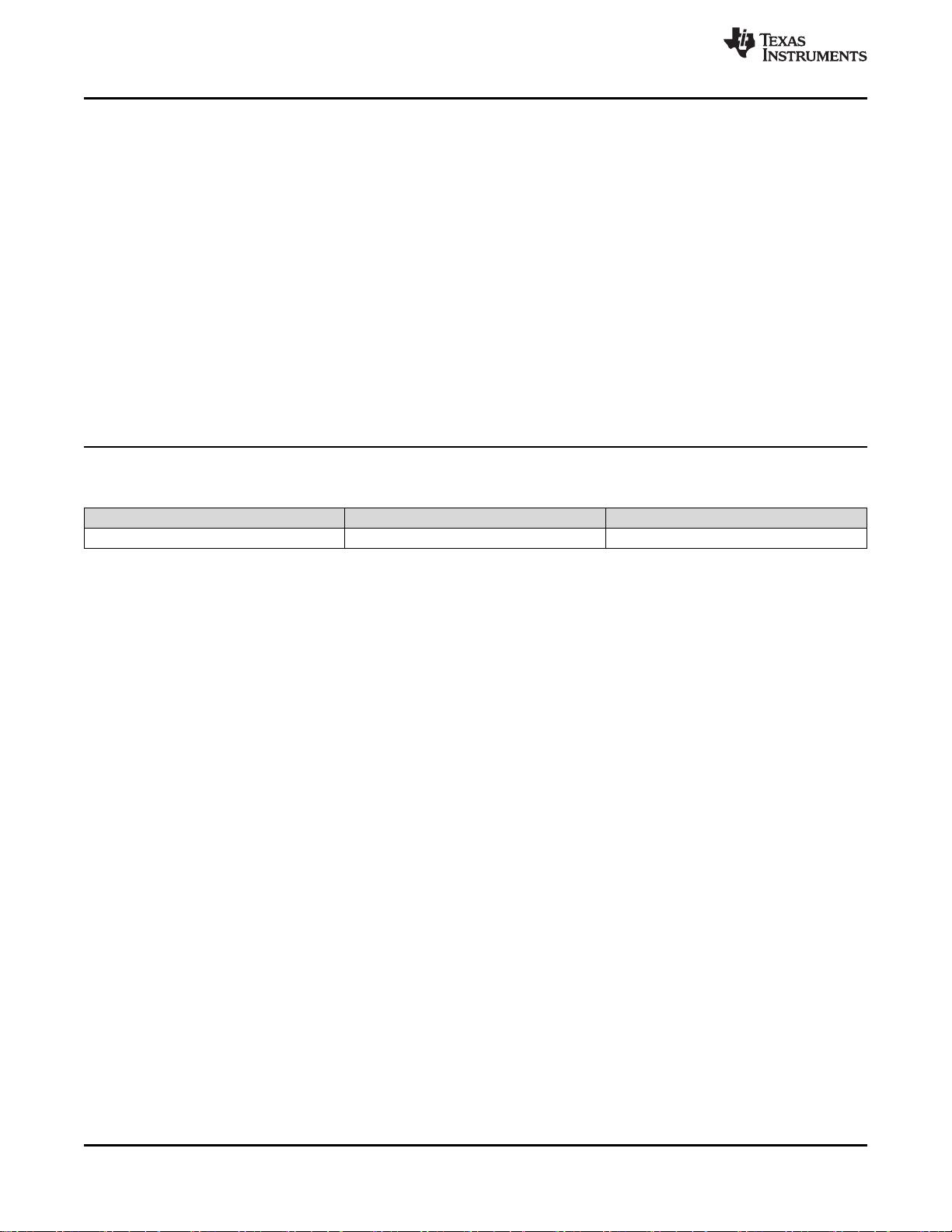
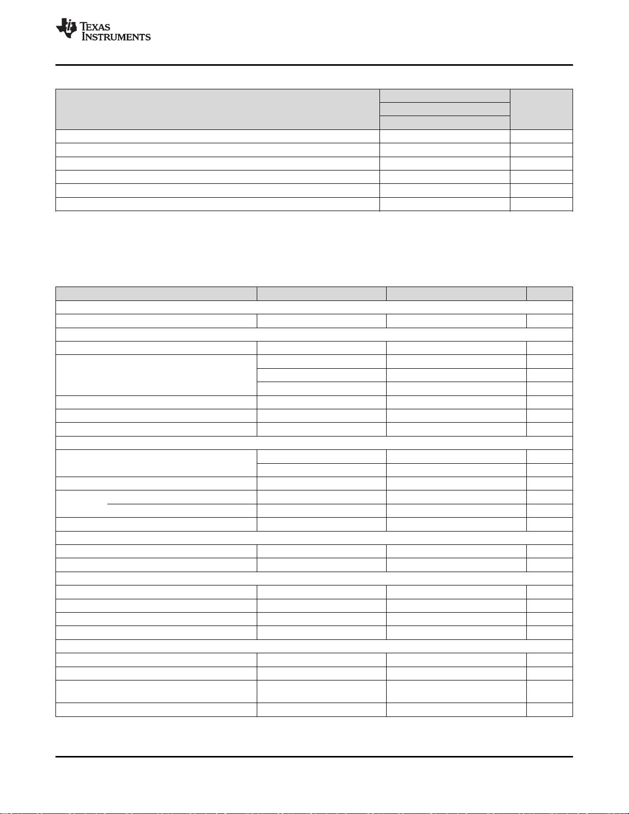
V
IN
(V)
Efficiency (%)
8 9 10 11 12 13 14 15 16 17 18
75
80
85
90
95
100
D019
V
O
= 60 V, I
LED
= 300 mA
TPS92691-Q1
1
2
3
4
5
6
7
8
16
15
14
13
12
11
10
9
VIN LED+
LEDÅ
VIN
SS
RT/SYNC
PWM
COMP
IADJ
IMON
AGND
PAD
VCC
GATE
IS
PGND
OVP
DDRV
CSP
CSN
L
R
OV1
R
OV2
R
IS
R
CS
Q
2
Q
1
D
C
SS
C
COMP
R
T
C
IMON
C
OUT
C
VCC
C
IN
C
OV
R
ADJ2
R
ADJ1
V
PWM
Product
Folder
Sample &
Buy
Technical
Documents
Tools &
Software
Support &
Community
An IMPORTANT NOTICE at the end of this data sheet addresses availability, warranty, changes, use in safety-critical applications,
intellectual property matters and other important disclaimers. PRODUCTION DATA.
English Data Sheet: SLVSD68
TPS92691
,
TPS92691-Q1
ZHCSEM9 –DECEMBER 2015
TPS92691/-Q1 具具有有轨轨到到轨轨电电流流感感测测放放大大器器的的多多拓拓扑扑 LED 驱驱动动器器
1
1 特特性性
1
• 宽输入电压范围:4.5V 至 65V
• 宽输出电压范围:2V 至 65V
• 低输入偏移轨到轨电流感测放大器
– 在 25°C 至 140°C 结温范围内,好于 ±3% 的发
光二极管 (LED) 电流精度
– 与高侧和低侧电流感测元件兼容
• 高阻抗模拟 LED 电流调节输入 (IADJ),对比度高
于 15:1
• 使用集成的串联 N 通道调光驱动器接口时,具有超
过 1000:1 串联场效应管 (FET) 脉宽调制 (PWM)
调光比率
• 具有 LED 电流持续监视输出用于系统故障检测和
诊断
• 可编程开关频率以实现与外部时钟同步
• 可编程软启动和斜坡补偿
• 综合故障保护电路,包括电源电压 (VCC) 欠压锁定
(UVLO)、输出过压保护 (OVP)、逐周期开关电流限
制和热保护
• TPS92691-Q1:符合汽车类 Q100 1 级标准
2 应应用用
• TPS92691-Q1:汽车外部照明 应用
• 建筑照明和通用照明 应用
3 说说明明
TPS92691/-Q1 是一款通用 LED 控制器,支持一系列
升压或降压驱动器拓扑。该器件实现了固定频率峰值电
流模式控制技术,可编程开关频率、斜坡补偿和软启动
时序。其整合了高电压 (65V) 轨到轨电流感测放大
器,从而可使用高侧或低侧串联感测电阻直接测量
LED 电流。该放大器可用于实现低输入偏移电压且在
25°C 至 140°C 结温范围和 0 至 60V 输出共模电压范
围获得好于 ±3% 的 LED 电流精度。
可使用模拟或 PWM 调光技术单独调制 LED 电流。通
过在高阻抗模拟调整输入 (IADJ) 范围内将电压从
140mV 改变为 2.25V 可获得具有 15:1 范围的线性模
拟调光响应。通过将 PWM 输入引脚调制为所需的占
空比和频率实现 LED 电流的 PWM 调光。可使用可选
DDRV 栅极驱动器输出使串联 FET 调光功能获得高于
1000:1 的对比度。
TPS92691/-Q1 支持通过电流监视输出连续检查 LED
状态。这样就可以实现 LED 短路或开路检测和保护。
其他故障保护 特性 包括 VCC UVLO、输出过压保护
(OVP)、开关逐周期电流限制和热保护。
器器件件信信息息
(1)
器器件件型型号号 封封装装 封封装装尺尺寸寸((标标称称值值))
TPS92691-Q1
TPS92691
HTSSOP (16) 5.10mm x 6.60mm
(1) 要了解所有可用封装,请参见数据表末尾的可订购产品附录。
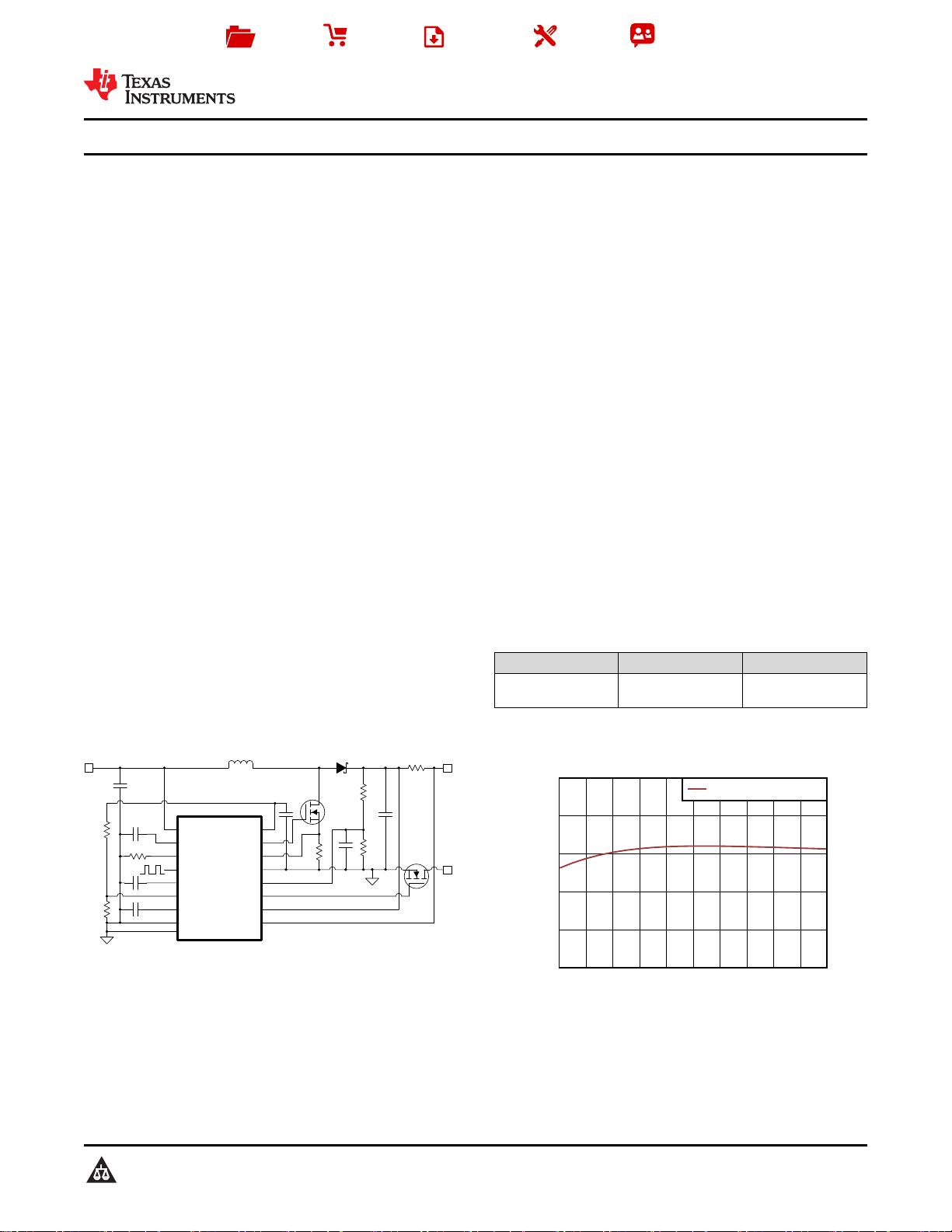
典典型型升升压压 LED 驱驱动动器器应应用用原原理理图图
效效率率与与输输出出电电压压之之间间的的关关系系
剩余45页未读,继续阅读
资源评论


