tps40345-mos管-电感-电容-数值计算
需积分: 5 176 浏览量
2022-05-23
17:43:27
上传
评论
收藏 2.43MB PDF 举报

5
4
3
2
6
7
8
9
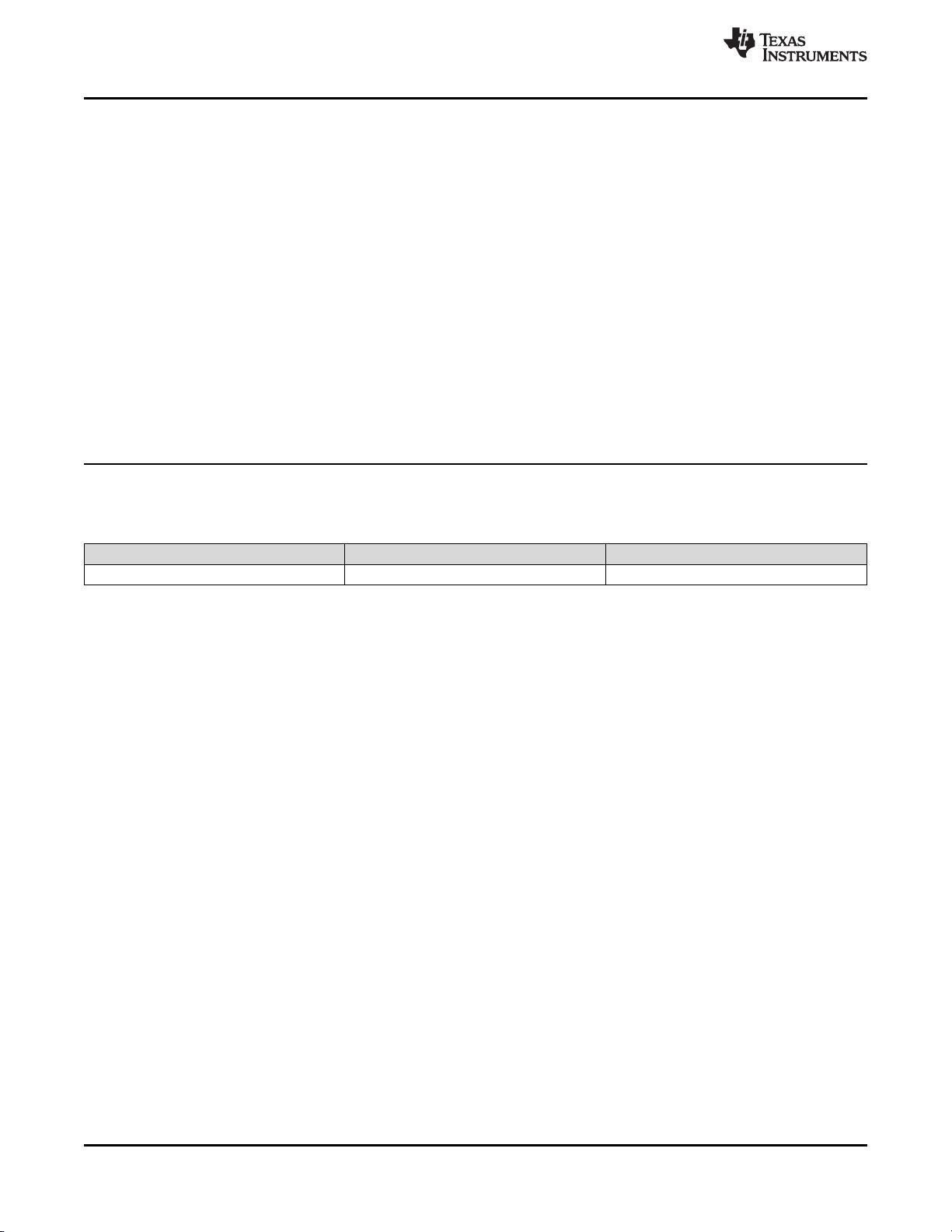
BOOT
HDRV
SW
LDRV/OC
FB
COMP
PGOOD
EN/SS
TPS40345
1 10BPVDD
PAD
V
IN
SD
V
OUT
V
IN
Copyright © 2017, Texas Instruments Incorporated
V
OUT
GND
Product
Folder
Order
Now
Technical
Documents
Tools &
Software
Support &
Community
An IMPORTANT NOTICE at the end of this data sheet addresses availability, warranty, changes, use in safety-critical applications,
intellectual property matters and other important disclaimers. PRODUCTION DATA.
English Data Sheet: SLUSD62
TPS40345
ZHCSH69 –DECEMBER 2017
TPS40345 3V 至至 20V 输输入入同同步步降降压压控控制制器器
1
1 特特性性
1
• 输入电压范围:3V 至 20V
• 600kHz 开关频率
• 高侧和低侧 FET R
DS(on)
电流检测
• 可编程热补偿 OCP 电平
• 可编程软启动
• 600mV、1.3% 基准电压
• 电压前馈补偿
• 支持预偏置输出
• 扩频频谱
• 145°C 的热关断保护限制
• 10 引脚 3mm × 3mm VSON 封装,散热垫具有接
地连接
2 应应用用
• 负载点 (POL) 模块
• 打印机
• 数字电视
• 电信
3 说说明明
TPS40345 是一款同步降压控制器,可在 3V 到 20V
的输入电压下工作,可用于成本优化型 应用。此控制
器实现了一种电压模式控制架构,具有输入电压前馈补
偿功能,可对输入电压变化做出即时响应。开关频率设
置为 600kHz。
开关频率中添加了扩频频谱 (FSS) 功能,显著降低了
峰值 EMI 噪声,使其更容易符合 EMI 标准。
TPS40345 可提供各种用户可编程功能,其中包括软
启动、过流保护 (OCP) 电平以及环路补偿。
OCP 电平可以通过从 LDRV 引脚连接到电路接地的单
个外部电阻器进行编程。在初始上电过程
中,TPS40345 可进入校准环节,测量 LDRV 引脚电
压,并设置内部 OCP 电压级。在工作期间,器件可在
通电时通过将已编程 OCP 电压电平与低侧 FET 上的
压降进行比较来确定是否发生过流情况。之
后,TPS40345 会进入关断和重启周期,直到故障消
除为止。
器器件件信信息息
(1)
器器件件型型号号 封封装装 封封装装尺尺寸寸((标标称称值值))
TPS40345 VSON (10) 3.00mm × 3.00mm
(1) 如需了解所有可用封装,请参阅数据表末尾的可订购产品附
录。
简简化化应应用用示示意意图图


剩余28页未读,继续阅读


评论0