没有合适的资源?快使用搜索试试~ 我知道了~
MSP430G2553手册
4星 · 超过85%的资源 需积分: 10 41 下载量 157 浏览量
2012-05-09
14:05:56
上传
评论 2
收藏 869KB PDF 举报
温馨提示
试读
69页
MSP430G2553手册,对MSP430G2553单片机进行了详细说明,包括内部结构功能及部分寄存器的详细说明。
资源推荐
资源详情
资源评论
MSP430G2x53
MSP430G2x13
www.ti.com
SLAS735E –APRIL 2011– REVISED JANUARY 2012
MIXED SIGNAL MICROCONTROLLER
1
FEATURES
• Low Supply-Voltage Range: 1.8 V to 3.6 V • Universal Serial Communication Interface
(USCI)
• Ultra-Low Power Consumption
– Enhanced UART Supporting Auto Baudrate
– Active Mode: 230 µA at 1 MHz, 2.2 V
Detection (LIN)
– Standby Mode: 0.5 µA
– IrDA Encoder and Decoder
– Off Mode (RAM Retention): 0.1 µA
– Synchronous SPI
• Five Power-Saving Modes
– I
2
C™
• Ultra-Fast Wake-Up From Standby Mode in
• On-Chip Comparator for Analog Signal
Less Than 1 µs
Compare Function or Slope Analog-to-Digital
• 16-Bit RISC Architecture, 62.5-ns Instruction
(A/D) Conversion
Cycle Time
• 10-Bit 200-ksps Analog-to-Digital (A/D)
• Basic Clock Module Configurations
Converter With Internal Reference,
– Internal Frequencies up to 16 MHz With
Sample-and-Hold, and Autoscan (See Table 1)
Four Calibrated Frequency
• Brownout Detector
– Internal Very-Low-Power Low-Frequency
• Serial Onboard Programming,
(LF) Oscillator
No External Programming Voltage Needed,
– 32-kHz Crystal
Programmable Code Protection by Security
– External Digital Clock Source
Fuse
• Two 16-Bit Timer_A With Three
• On-Chip Emulation Logic With Spy-Bi-Wire
Capture/Compare Registers
Interface
• Up to 24 Touch-Sense-Enabled I/O Pins
• Family Members are Summarized in Table 1
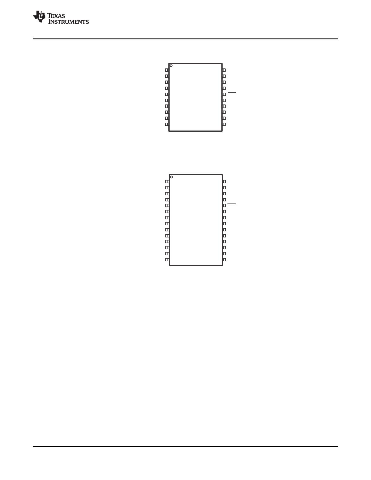
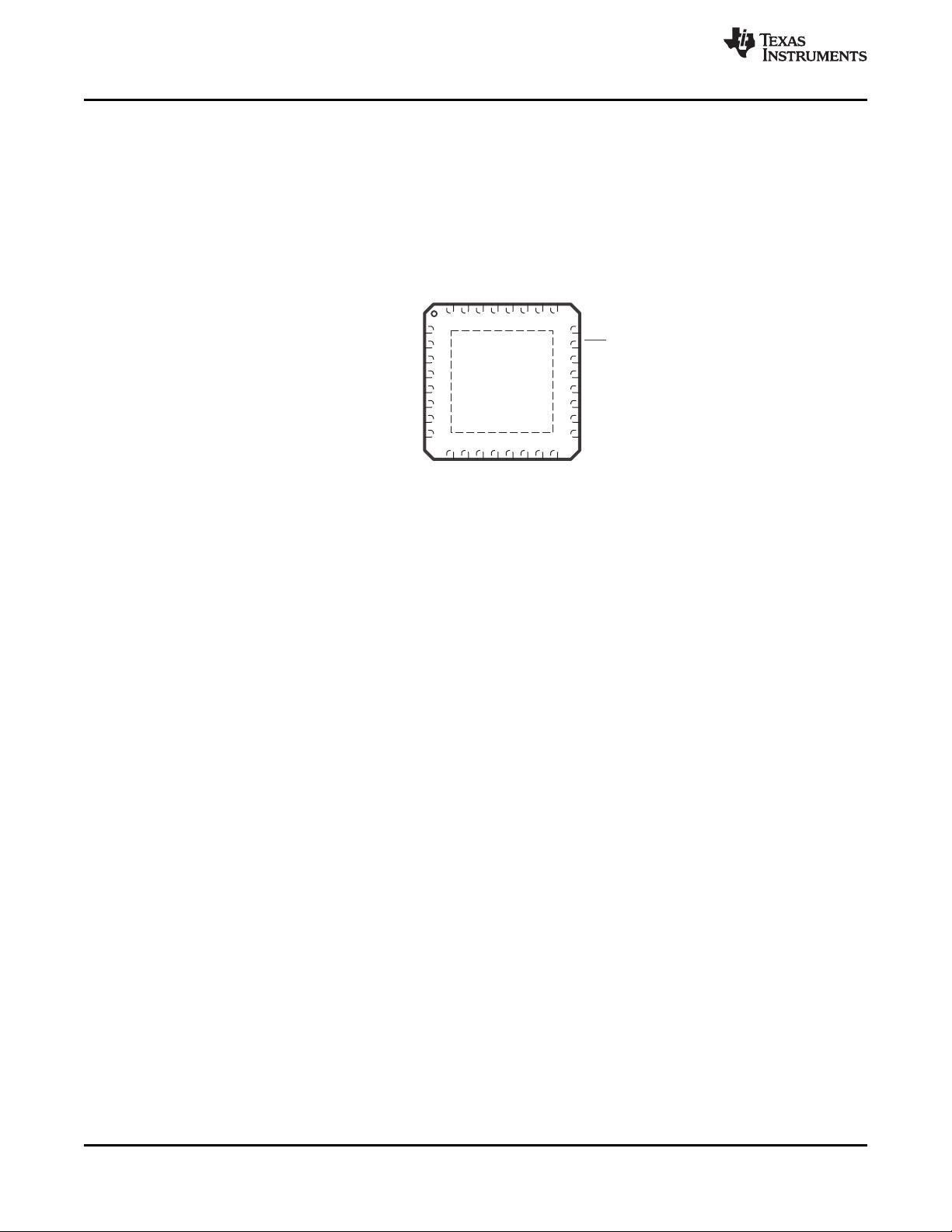
• Package Options
– TSSOP: 20 Pin, 28 Pin
– PDIP: 20 Pin
– QFN: 32 Pin
• For Complete Module Descriptions, See the
MSP430x2xx Family User’s Guide (SLAU144)
DESCRIPTION
The Texas Instruments MSP430 family of ultra-low-power microcontrollers consists of several devices featuring
different sets of peripherals targeted for various applications. The architecture, combined with five low-power
modes, is optimized to achieve extended battery life in portable measurement applications. The device features a
powerful 16-bit RISC CPU, 16-bit registers, and constant generators that contribute to maximum code efficiency.
The digitally controlled oscillator (DCO) allows wake-up from low-power modes to active mode in less than 1 µs.
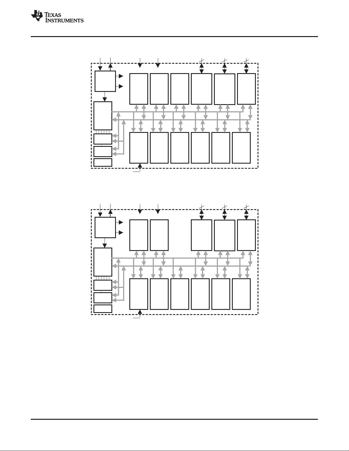
The MSP430G2x13 and MSP430G2x53 series are ultra-low-power mixed signal microcontrollers with built-in
16-bit timers, up to 24 I/O touch-sense-enabled pins, a versatile analog comparator, and built-in communication
capability using the universal serial communication interface. In addition the MSP430G2x53 family members
have a 10-bit analog-to-digital (A/D) converter. For configuration details see Table 1.
Typical applications include low-cost sensor systems that capture analog signals, convert them to digital values,
and then process the data for display or for transmission to a host system.
1
Please be aware that an important notice concerning availability, standard warranty, and use in critical applications of Texas
Instruments semiconductor products and disclaimers thereto appears at the end of this data sheet.
PRODUCTION DATA information is current as of publication date.
Copyright © 2011–2012, Texas Instruments Incorporated
Products conform to specifications per the terms of the Texas
Instruments standard warranty. Production processing does not
necessarily include testing of all parameters.
MSP430G2x53
MSP430G2x13
SLAS735E –APRIL 2011– REVISED JANUARY 2012
www.ti.com
Table 1. Available Options
(1)(2)
Flash RAM COMP_A+ ADC10 USCI Package
Device BSL EEM Timer_A Clock I/O
(KB) (B) Channel Channel A0/B0 Type
MSP430G2553IRHB32 24 32-QFN
LF,
MSP430G2553IPW28 24 28-TSSOP
1 1 16 512 2x TA3 8 8 1 DCO,
MSP430G2553IPW20 16 20-TSSOP
VLO
MSP430G2553IN20 16 20-PDIP
MSP430G2453IRHB32 24 32-QFN
LF,
MSP430G2453IPW28 24 28-TSSOP
1 1 8 512 2x TA3 8 8 1 DCO,
MSP430G2453IPW20 16 20-TSSOP
VLO
MSP430G2453IN20 16 20-PDIP
MSP430G2353IRHB32 24 32-QFN
LF,
MSP430G2353IPW28 24 28-TSSOP
1 1 4 256 2x TA3 8 8 1 DCO,
MSP430G2353IPW20 16 20-TSSOP
VLO
MSP430G2353IN20 16 20-PDIP
MSP430G2253IRHB32 24 32-QFN
LF,
MSP430G2253IPW28 24 28-TSSOP
1 1 2 256 2x TA3 8 8 1 DCO,
MSP430G2253IPW20 16 20-TSSOP
VLO
MSP430G2253IN20 16 20-PDIP
MSP430G2153IRHB32 24 32-QFN
LF,
MSP430G2153IPW28 24 28-TSSOP
1 1 1 256 2x TA3 8 8 1 DCO,
MSP430G2153IPW20 16 20-TSSOP
VLO
MSP430G2153IN20 16 20-PDIP
MSP430G2513IRHB32 24 32-QFN
LF,
MSP430G2513IPW28 24 28-TSSOP
1 1 16 512 2x TA3 8 - 1 DCO,
MSP430G2513IPW20 16 20-TSSOP
VLO
MSP430G2513IN20 16 20-PDIP
MSP430G2413IRHB32 24 32-QFN
LF,
MSP430G2413IPW28 24 28-TSSOP
1 1 8 512 2x TA3 8 - 1 DCO,
MSP430G2413IPW20 16 20-TSSOP
VLO
MSP430G2413IN20 16 20-PDIP
MSP430G2313IRHB32 24 32-QFN
LF,
MSP430G2313IPW28 24 28-TSSOP
1 1 4 256 2x TA3 8 - 1 DCO,
MSP430G2313IPW20 16 20-TSSOP
VLO
MSP430G2313IN20 16 20-PDIP
MSP430G2213IRHB32 24 32-QFN
LF,
MSP430G2213IPW28 24 28-TSSOP
1 1 2 256 2x TA3 8 - 1 DCO,
MSP430G2213IPW20 16 20-TSSOP
VLO
MSP430G2213IN20 16 20-PDIP
MSP430G2113IRHB32 24 32-QFN
LF,
MSP430G2113IPW28 24 28-TSSOP
1 1 1 256 2x TA3 8 - 1 DCO,
MSP430G2113IPW20 16 20-TSSOP
VLO
MSP430G2113IN20 16 20-PDIP
(1) For the most current package and ordering information, see the Package Option Addendum at the end of this document, or see the TI
web site at www.ti.com.
(2) Package drawings, thermal data, and symbolization are available at www.ti.com/packaging.
2 Submit Documentation Feedback Copyright © 2011–2012, Texas Instruments Incorporated
N20
PW20
(TOP VIEW)
1DVCC
2P1.0/TA0CLK/ACLK/A0/CA0
3
4
5P1.3/ADC10CLK/CAOUT/VREF-/VEREF-/A3/CA3
6
7
8P2.0/TA1.0
9P2.1/TA1.1
10P2.2/TA1.1 11 P2.3/TA1.0
12 P2.4/TA1.2
13 P2.5/TA1.2
14
15
16 RST/NMI/SBWTDIO
17 TEST/SBWTCK
18 XOUT/P2.7
19 XIN/P2.6/TA0.1
20 DVSS
P1.6/TA0.1/ CA6/TDI/TCLKUCB0SOMI/UCB0SCL/A6/
P1.7/CAOUT /A7/CA7/TDO/TDI/UCB0SIMO/UCB0SDA
P1.1/TA0.0/ A1/CA1/UCA0RXD/UCA0SOMI
P1.2/TA0.1/ A2/CA2/UCA0TXD/PUCA0SIMO
P1.4/SMCLK/ CA4/TCK/VREF+/VEREF+/A4/UCB0STE/UCA0CLK
P1.5/TA0.0/ A5/CA5/TMS/UCB0CLK/UCA0STE
PW28
(TOP VIEW)
1DVCC
2P1.0/TA0CLK/ACLK/A0/CA0
3
4
5P1.3/ADC10CLK/CAOUT/VREF-/VEREF-/A3/CA3
6
7
8
P3.0/TA0.2
9
P3.1/TA1.0
10P2.0/TA1.0 19 P3.5/TA0.1
20 P3.6/TA0.2
21 P3.7/TA1CLK/CAOUT
22
23
24 RST/NMI/SBWTDIO
25 TEST/SBWTCK
26 XOUT/P2.7
27 XIN/P2.6/TA0.1
28 DVSS
P1.6/TA0.1/ CA6/TDI/TCLKUCB0SOMI/UCB0SCL/A6/
P1.7/CAOUT /A7/CA7/TDO/TDI/UCB0SIMO/UCB0SDA
P1.1/TA0.0/ A1/CA1/UCA0RXD/UCA0SOMI
P1.2/TA0.1/ A2/CA2/UCA0TXD/PUCA0SIMO
P1.4/SMCLK/ CA4/TCK/VREF+/VEREF+/A4/UCB0STE/UCA0CLK
P1.5/TA0.0/ A5/CA5/TMS/UCB0CLK/UCA0STE
11
12P2.2/TA1.1
13P3.2/TA1.1
14P3.3/TA1.2 15 P3.4/TA0.0
16 P2.3/TA1.0
17 P2.4/TA1.2
18
P2.5/TA1.2
P2.1/TA1.1
MSP430G2x53
MSP430G2x13
www.ti.com
SLAS735E –APRIL 2011– REVISED JANUARY 2012
Device Pinout, MSP430G2x13 and MSP430G2x53, 20-Pin Devices, TSSOP and PDIP
NOTE: ADC10 is available on MSP430G2x53 devices only.
NOTE: The pulldown resistors of port P3 should be enabled by setting P3REN.x = 1.
Device Pinout, MSP430G2x13 and MSP430G2x53, 28-Pin Devices, TSSOP
NOTE: ADC10 is available on MSP430G2x53 devices only.
Copyright © 2011–2012, Texas Instruments Incorporated Submit Documentation Feedback 3
RHB32
(TOP VIEW)
1
2
3
4
5
6
P2.0/TA1.0
7
P2.1/TA1.1
8NC
9
P2.2/TA1.1
10
P3.0/TA0.2
11
P3.1/TA1.0
12
P3.2/TA1.1
13
P3.3/TA1.2
14
P3.4/TA0.0
15
P3.5/TA0.1
16
P2.3/TA1.0
17
P2.4/TA1.2
18
P2.5/TA1.2
19
20
P3.6/TA0.2
21
P3.7/TA1CLK/CAOUT
22
23 RST/NMI/SBWTDIO
24 TEST/SBWTCK
25
XOUT/P2.7
26
XIN/P2.6/TA0.1
27
AVSS
28
DVSS
29
AVCC
30
DVCC
31
P1.0/TA0CLK/ACLK/A0/CA0
32
NC
P1.3/ADC10CLK/CAOUT/VREF-/VEREF-/A3/CA3
P1.1/TA0.0/ A1/CA1/
UCA0RXD/UCA0SOMI
P1.2/TA0.1/ A2/CA2/UCA0TXD/UCA0SIMO
P1.4/SMCLK/ CA4/TCK/VREF+/VEREF+/A4/UCB0STE/UCA0CLK
P1.5/TA0.0/ A5/CA5/TMS/UCB0CLK/UCA0STE
P1.6/TA0.1/ CA6/TDI/TCLKUCB0SOMI/UCB0SCL/A6/
P1.7/CAOUT /CA7/TDO/TDI/UCB0SIMO/UCB0SDA/A7
MSP430G2x53
MSP430G2x13
SLAS735E –APRIL 2011– REVISED JANUARY 2012
www.ti.com
Device Pinout, MSP430G2x13 and MSP430G2x53, 32-Pin Devices, QFN
NOTE: ADC10 is available on MSP430G2x53 devices only.
4 Submit Documentation Feedback Copyright © 2011–2012, Texas Instruments Incorporated
Clock
System
Brownout
Protection
RST/NMI
DVCC DVSS
MCLK
Watchdog
WDT+
15-Bit
Timer0_A3
3 CC
Registers
16MHz
CPU
incl. 16
Registers
Emulation
2BP
JTAG
Interface
SMCLK
ACLK
MDB
MAB
Port P1
8 I/O
Interrupt
capability
pullup/down
resistors
P1.x
8
P2.x
Port P2
8 I/O
Interrupt
capability
pullup/down
resistors
Spy-Bi-
Wire
Comp_A+
8 Channels
Timer1_A3
3 CC
Registers
XIN XOUT
Port P3
8 I/O
pullup/
pulldown
resistors
P3.x
8 8
RAM
512B
256B
Flash
16KB
8KB
4KB
2KB
USCI A0
UART/
LIN, IrDA,
SPI
USCI B0
SPI, I2C
ADC
10-Bit
8 Ch.
Autoscan
1 ch DMA
Clock
System
Brownout
Protection
RST/NMI
DVCC DVSS
MCLK
Watchdog
WDT+
15-Bit
Timer0_A3
3 CC
Registers
16MHz
CPU
incl. 16
Registers
Emulation
2BP
JTAG
Interface
SMCLK
ACLK
Port P1
8 I/O
Interrupt
capability
pullup/down
resistors
P1.x
8
P2.x
Port P2
8 I/O
Interrupt
capability
pullup/down
resistors
Spy-Bi-
Wire
Comp_A+
8 Channels
Timer1_A3
3 CC
Registers
XIN XOUT
Port P3
8 I/O
pullup/
pulldown
resistors
P3.x
8 8
RAM
512B
256B
Flash
16KB
8KB
4KB
2KB
USCI A0
UART/
LIN, IrDA,
SPI
USCI B0
SPI, I2C
MDB
MAB
MSP430G2x53
MSP430G2x13
www.ti.com
SLAS735E –APRIL 2011– REVISED JANUARY 2012
Functional Block Diagram, MSP430G2x53
NOTE: Port P3 is available on 28-pin and 32-pin devices only.
Functional Block Diagram, MSP430G2x13
NOTE: Port P3 is available on 28-pin and 32-pin devices only.
Copyright © 2011–2012, Texas Instruments Incorporated Submit Documentation Feedback 5
剩余68页未读,继续阅读
赵泽奇
- 粉丝: 0
- 资源: 2
上传资源 快速赚钱
- 我的内容管理 展开
- 我的资源 快来上传第一个资源
- 我的收益 登录查看自己的收益
- 我的积分 登录查看自己的积分
- 我的C币 登录后查看C币余额
- 我的收藏
- 我的下载
- 下载帮助
安全验证
文档复制为VIP权益,开通VIP直接复制
信息提交成功
- 1
- 2
前往页