

SPRS226M − NOVEMBER 2003 − REVISED APRIL 2009
1
POST OFFICE BOX 1443 • HOUSTON, TEXAS 77251−1443
Highest-Performance Fixed-Point DSPs
− 1.67-/1.39-/1.17-/1-ns Instruction Cycle
− 600-/720-/850-MHz, 1-GHz Clock Rate
− Eight 32-Bit Instructions/Cycle
− Twenty-Eight Operations/Cycle
− 4800, 5760, 6800, 8000 MIPS
− Fully Software-Compatible With C62x
− C6414/15/16 Devices Pin-Compatible
− Extended Temperature Devices Available
VelociTI.2 Extensions to VelociTI
Advanced Very-Long-Instruction-Word
(VLIW) TMS320C64x DSP Core
− Eight Highly Independent Functional
Units With VelociTI.2 Extensions:
− Six ALUs (32-/40-Bit), Each Supports
Single 32-Bit, Dual 16-Bit, or Quad
8-Bit Arithmetic per Clock Cycle
− Two Multipliers Support
Four 16 x 16-Bit Multiplies
(32-Bit Results) per Clock Cycle or
Eight 8 x 8-Bit Multiplies
(16-Bit Results) per Clock Cycle
− Non-Aligned Load-Store Architecture
− 64 32-Bit General-Purpose Registers
− Instruction Packing Reduces Code Size
− All Instructions Conditional
Instruction Set Features
− Byte-Addressable (8-/16-/32-/64-Bit Data)
− 8-Bit Overflow Protection
− Bit-Field Extract, Set, Clear
− Normalization, Saturation, Bit-Counting
− VelociTI.2 Increased Orthogonality
VCP [C6416T Only]
− Supports Over 833 7.95-Kbps AMR
− Programmable Code Parameters
TCP [C6416T Only]
− Supports up to 10 2-Mbps or
60 384-Kbps 3GPP (6 Iterations)
− Programmable Turbo Code and
Decoding Parameters
L1/L2 Memory Architecture
− 128K-Bit (16K-Byte) L1P Program Cache
(Direct Mapped)
− 128K-Bit (16K-Byte) L1D Data Cache
(2-Way Set-Associative)
− 8M-Bit (1024K-Byte) L2 Unified Mapped
RAM/Cache (Flexible Allocation)
Two External Memory Interfaces (EMIFs)
− One 64-Bit (EMIFA), One 16-Bit (EMIFB)
− Glueless Interface to Asynchronous
Memories (SRAM and EPROM) and
Synchronous Memories (SDRAM,
SBSRAM, ZBT SRAM, and FIFO)
− 1280M-Byte Total Addressable External
Memory Space
Enhanced Direct-Memory-Access (EDMA)
Controller (64 Independent Channels)
Host-Port Interface (HPI)
− User-Configurable Bus Width (32-/16-Bit)
32-Bit/33-MHz, 3.3-V PCI Master/Slave
Interface Conforms to PCI Specification 2.2
[C6415T/C6416T]
− Three PCI Bus Address Registers:
Prefetchable Memory
Non-Prefetchable Memory I/O
− Four-Wire Serial EEPROM Interface
− PCI Interrupt Request Under DSP
Program Control
− DSP Interrupt Via PCI I/O Cycle
Three Multichannel Buffered Serial Ports
− Direct Interface to T1/E1, MVIP, SCSA
Framers
− Up to 256 Channels Each
− ST-Bus-Switching-, AC97-Compatible
− Serial Peripheral Interface (SPI)
Compatible (Motorola)
Three 32-Bit General-Purpose Timers
UTOPIA [C6415T/C6416T]
− UTOPIA Level 2 Slave ATM Controller
− 8-Bit Transmit and Receive Operations
up to 50 MHz per Direction
− User-Defined Cell Format up to 64 Bytes
Sixteen General-Purpose I/O (GPIO) Pins
Flexible PLL Clock Generator
IEEE-1149.1 (JTAG
†
)
Boundary-Scan-Compatible
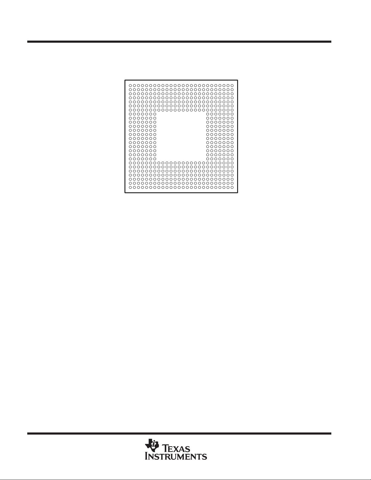
532-Pin Ball Grid Array (BGA) Package
(GLZ/ZLZ/CLZ Suffixes), 0.8-mm Ball Pitch
0.09-µm/7-Level Cu Metal Process (CMOS)
3.3-V I/Os, 1.1-V Internal (600 MHz)
3.3-V I/Os, 1.2-V Internal (720/850 MHZ, 1
GHz)
Please be aware that an important notice concerning availability, standard warranty, and use in critical applications o
f
Texas Instruments semiconductor products and disclaimers thereto appears at the end of this data sheet.
!"# $ %&'# "$ (&)*%"# +"#',
+&%#$ %! # $('%%"#$ (' #-' #'!$ '."$ $#&!'#$
$#"+"+ /""#0, +&%# (%'$$1 +'$ # '%'$$"*0 %*&+'
#'$#1 "** (""!'#'$,
Copyright 2009, Texas Instruments Incorporated
C62x, VelociTI.2, VelociTI, and TMS320C64x are trademarks of Texas Instruments.
Motorola is a trademark of Motorola, Inc.
†
IEEE Standard 1149.1-1990 Standard-Test-Access Port and Boundary Scan Architecture.