没有合适的资源?快使用搜索试试~ 我知道了~
如何利用AI提高内容生产
资源推荐
资源详情
资源评论
HFC
CMOS Introduction and Application
Device Technology
Jianhua Ju
Oct, 2022
HFC
Outline
• Semiconductor material
• PN junction
• MOS capacitance
• MOSFET
• CMOS and application
• Inverter
• SRAM
• RO
• Summary
HFC
Outline
• Semiconductor material
• Conductor, Semiconductor and Insulator
• Intrinsic semiconductor, N-type and P-type semiconductor
• Semiconductor Energy bend and Feimi level
• PN junction
• MOS capacitance
• MOSFET
• CMOS and application
• Inverter
• SRAM
• RO
• Summary
HFC
Semiconductor Material
One atom
Two atoms
Electron in crystal, E-Level E-Band
• From Atomic level to solid Energy-Band
• From Carbon atom E-level to Diamond crystal E-band formation
5.43A
6N States
2N electrons
3P
3S
2N States
2N electrons
4N States
0N electron
4N States
4N electrons
Conduction Band
Valence Band
Distance between Carbon in crystal
Eg
Ec
Ev
HFC
• Solid material divide into three classes: Conductor, Semiconductor and Insulator
• Conductor has two type band:
Type I conduction band half occupied by electrons
Type II conduction-valence band has overlapped, electrons can’t occupy all the band
• Semiconductor band:
There is a energy gap between conduction & valence band, the gap is smaller
• Insulator band:
The Gap is so large that electron can’t be excited by thermal from valence to conduction band
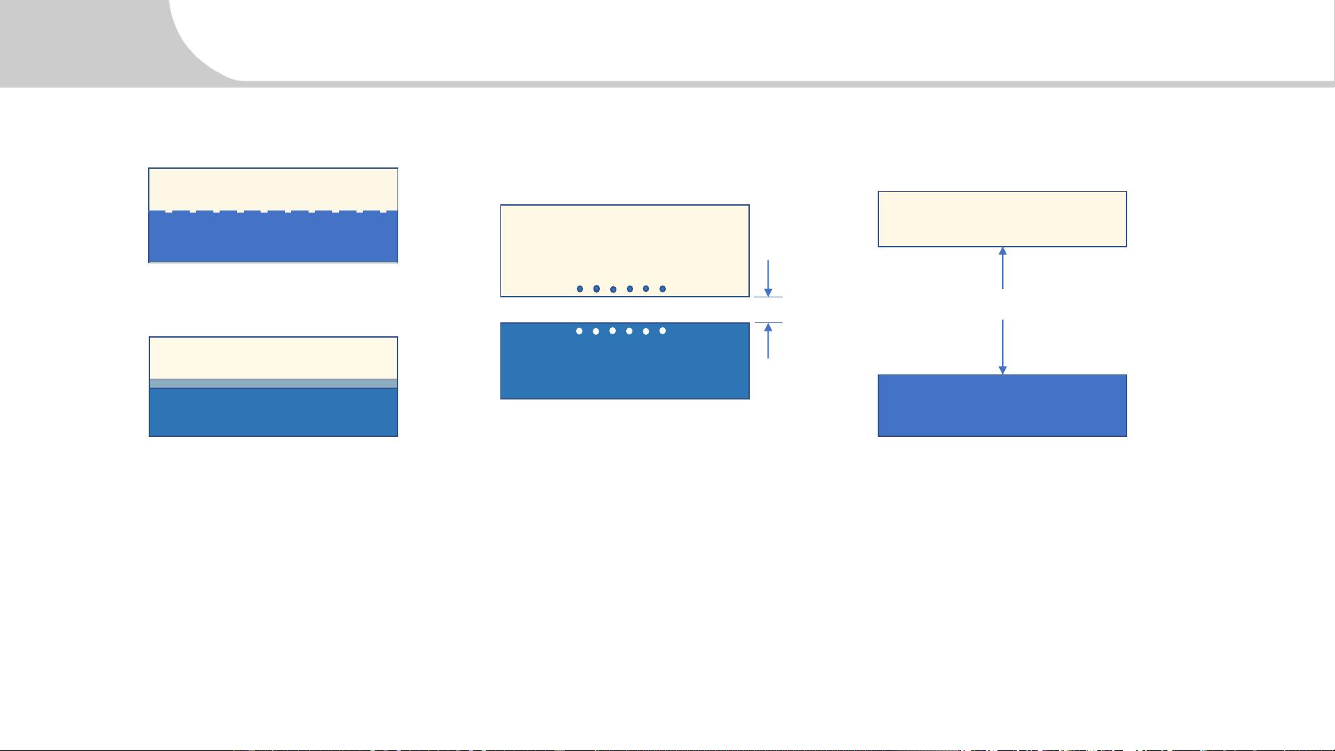
Conductor Semiconductor Insulator
Conduction band electron half filled
Conduction-Valence band overlap
Valence band
with a few holes
Conduction band
with a few electrons
Empty Conduction Band
Full occupied Valence Band
Eg ~ 1eV
Eg ~ 9 eV
Semiconductor Material
剩余41页未读,继续阅读
资源评论
zthYH
- 粉丝: 30
- 资源: 4
上传资源 快速赚钱
- 我的内容管理 展开
- 我的资源 快来上传第一个资源
- 我的收益 登录查看自己的收益
- 我的积分 登录查看自己的积分
- 我的C币 登录后查看C币余额
- 我的收藏
- 我的下载
- 下载帮助
安全验证
文档复制为VIP权益,开通VIP直接复制
信息提交成功