没有合适的资源?快使用搜索试试~ 我知道了~
硬件之光实战篇-Boost
0 下载量 98 浏览量
2024-01-09
09:54:25
上传
评论
收藏 256KB PDF 举报
温馨提示
试读
11页
MP1541-Datasheet
资源推荐
资源详情
资源评论
MP1541
1.3MHz Boost Converter
MP1541 Rev.1.5 www.MonolithicPower.com 1
9/5/2017 MPS Proprietary Information. Patent Protected. Unauthorized Photocopy and Duplication Prohibited.
© 2017 MPS. All Rights Reserved.
The Future of Analog IC Technology
DESCRIPTION
The MP1541 is a current mode step up
converter intended for small, low power
applications. The MP1541 switches at 1.3MHz
and allows the use of tiny, low cost capacitors
and inductors 2mm or less in height. Internal
soft start results in small inrush current and
extends battery life. The MP1541 operates from
an input voltage as low as 2.5V and can
generate 12V at up to 300mA from a 5V supply.
The MP1541 includes under-voltage lockout,
current limiting, and thermal overload protection
to prevent damage in the event of an output
overload. The MP1541 is available in a small
5-pin TSOT23 package or QFN-8 (2mmX2mm)
package.
FEATURES
On Board Power MOSFET
Uses Tiny Capacitors and Inductors
1.3MHz Fixed Switching Frequency
Internally Compensated
Internal Soft-Start
Operates with Input Voltage as Low as 2.5V
and Output Voltage as High as 22V
12V at 300mA from 5V Input
UVLO, Thermal Shutdown
Internal Current Limit
Available in a TSOT23-5 Package or QFN-8
(2mmX2mm) Package
APPLICATIONS
Camera Phone Flash
Handheld Computers and PDAs
Digital Still and Video Cameras
External Modems
Small LCD Displays
White LED Driver
A
ll MPS parts are lead-free, halogen free, and adhere to the RoHS directive. Fo
r
MPS green status, please visit MPS website under Quality Assurance. “MPS”
and “The Future of Analog IC Technology” are Registered Trademarks o
f
Monolithic Power Systems, Inc.
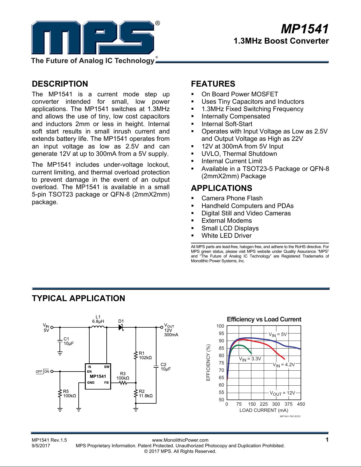
TYPICAL APPLICATION
100
95
90
85
80
75
70
65
60
55
50
EFFICIENCY (%)
0 75 150 225 300 375 450
LOAD CURRENT (mA)
MP1541-TAC-EC01
Efficiency vs Load Current
V
IN
= 3.3V
V
IN
= 5V
V
OUT
= 12V
V
IN
= 4.2V
MP1541 – 1.3MHz BOOST CONVERTER
MP1541 Rev.1.5 www.MonolithicPower.com 2
9/5/2017 MPS Proprietary Information. Patent Protected. Unauthorized Photocopy and Duplication Prohibited.
© 2017 MPS. All Rights Reserved.
ORDERING INFORMATION
Part Number Package Top Marking
MP1541DJ* TSOT23-5
See Below
MP1541GG** QFN-8 (2mmX2mm)
* For Tape & Reel, add suffix –Z (e.g. MP1541DJ–Z)
For RoHS compliant packaging, add suffix –LF (e.g. MP1541DJ–LF–Z)
** For Tape & Reel, add suffix –Z (e.g. MP1541GG–Z)
TOP MARKING
(MP1541DJ)
B3: product code of MP1541DJ
Y: year code
W: week code
TOP MARKING
(MP1541GG)
GV: product code of MP1541GG
Y: year code
LLL: lot number
MP1541 – 1.3MHz BOOST CONVERTER
MP1541 Rev.1.5 www.MonolithicPower.com 3
9/5/2017 MPS Proprietary Information. Patent Protected. Unauthorized Photocopy and Duplication Prohibited.
© 2017 MPS. All Rights Reserved.
PACKAGE REFERENCE
TOP VIEW
B3YW
SW
GND
FB
1
2
3
5
4
IN
EN
TSOT23-5 QFN-8 (2mmX2mm)
ABSOLUTE MAXIMUM RATINGS
(1)
SW Pin ........................................... –0.3V to 25V
All Other Pins ................................ –0.3V to 6.5V
Junction Temperature ............................... 150°C
Continuous Power Dissipation (T
A
= +25°C)
(2)
TSOT23-5 ................................................ 0.47W
QFN-8 (2mmx2mm) ................................. 1.56W
Lead Temperature .................................... 260°C
Storage Temperature .............. –65°C to +150°C
Recommended Operating Conditions
(3)
Supply Voltage V
IN
............................. 2.5V to 6V
Output Voltage V
OUT
............................ 3V to 22V
Operating Temperature............. –40°C to +85°C
Maximum Junction Temp. (T
J
) ............. +125°C
Thermal Resistance
(4)
θ
JA
θ
JC
TSOT25 ................................. 220 .... 110 .. C/W
QFN-8 (2mmX2mm) ............... 80 ...... 16 ... C/W
Notes:
1) Exceeding these ratings may damage the device.
2) The maximum allowable power dissipation is a function of the
maximum junction temperature T
J
(MAX), the junction-to-
ambient thermal resistance θ
JA
, and the ambient temperature
T
A
. The maximum allowable continuous power dissipation at
any ambient temperature is calculated by P
D
(MAX)=(T
J
(MAX)-
T
A
)/θ
JA
. Exceeding the maximum allowable power dissipation
will cause excessive die temperature, and the regulator will go
into thermal shutdown. Internal thermal shutdown circuitry
protects the device from permanent damage.
3) The device is not guaranteed to function outside of its
operating range.
4) Measured on JESD51-7 4-layer board.
剩余10页未读,继续阅读
资源评论
展翅大黄蜂
- 粉丝: 98
- 资源: 1
上传资源 快速赚钱
- 我的内容管理 展开
- 我的资源 快来上传第一个资源
- 我的收益 登录查看自己的收益
- 我的积分 登录查看自己的积分
- 我的C币 登录后查看C币余额
- 我的收藏
- 我的下载
- 下载帮助
安全验证
文档复制为VIP权益,开通VIP直接复制
信息提交成功