没有合适的资源?快使用搜索试试~ 我知道了~
音频解码芯片ES8388 数据手册
资源推荐
资源详情
资源评论
Low Power Stereo Audio CODEC
With Headphone Amplifier
Revision 12.0 November 2023
Latest datasheet: www.everest-semi.com
or info@everest-semi.com
1
ES8388
GENERAL DESCRIPTION
FEATURES
ES8388 is a high performance, low
power and low cost audio CODEC.
It consists of 2-ch ADC, 2-ch DAC,
microphone amplifier, headphone
amplifier, digital sound effects, and
analog mixing and gain functions.
The device uses advanced multi-bit
delta-sigma modulation technique
to convert data between digital and
analog. The multi-bit delta-sigma
modulators make the device with
low sensitivity to clock jitter and low
out of band noise.
ADC
• 24-bit, 8 kHz to 96 kHz sampling frequency
• 95 dB dynamic range, 95 dB signal to noise ratio,
-85 dB THD+N
• Stereo or mono microphone interface with
microphone amplifier
• Auto level control and noise gate
• 2-to-1 analog input selection
• Various analog input mixing and gains
DAC
• 24-bit, 8 kHz to 96 kHz sampling frequency
• 96 dB dynamic range, 96 dB signal to noise ratio,
-83 dB THD+N
• 40 mW headphone amplifier, pop noise free
• Headphone capless mode
• Stereo enhancement
• Bass and Treble
• Various analog output mixing and gains
Low Power
• 1.8V to 3.3V operation
• 7 mW playback; 16 mW playback and record
System
• I
2
C or SPI uC interface
• 256Fs, 384Fs, USB 12 MHz or 24 MHz
• Master or slave serial port
• I
2
S, Left Justified, DSP/PCM Mode
APPLICATIONS
ORDERING INFORMATION
• MID
• MP3, MP4, PMP
• Wireless audio
• Digital camera, camcorder
• GPS
• Bluetooth
• Portable audio devices
ES8388 -40°C ~ +85°C
QFN-28
Everest Semiconductor ES8388
Revision 12.0 November 2023
Latest datasheet: www.everest-semi.com
or info@everest-semi.com
2
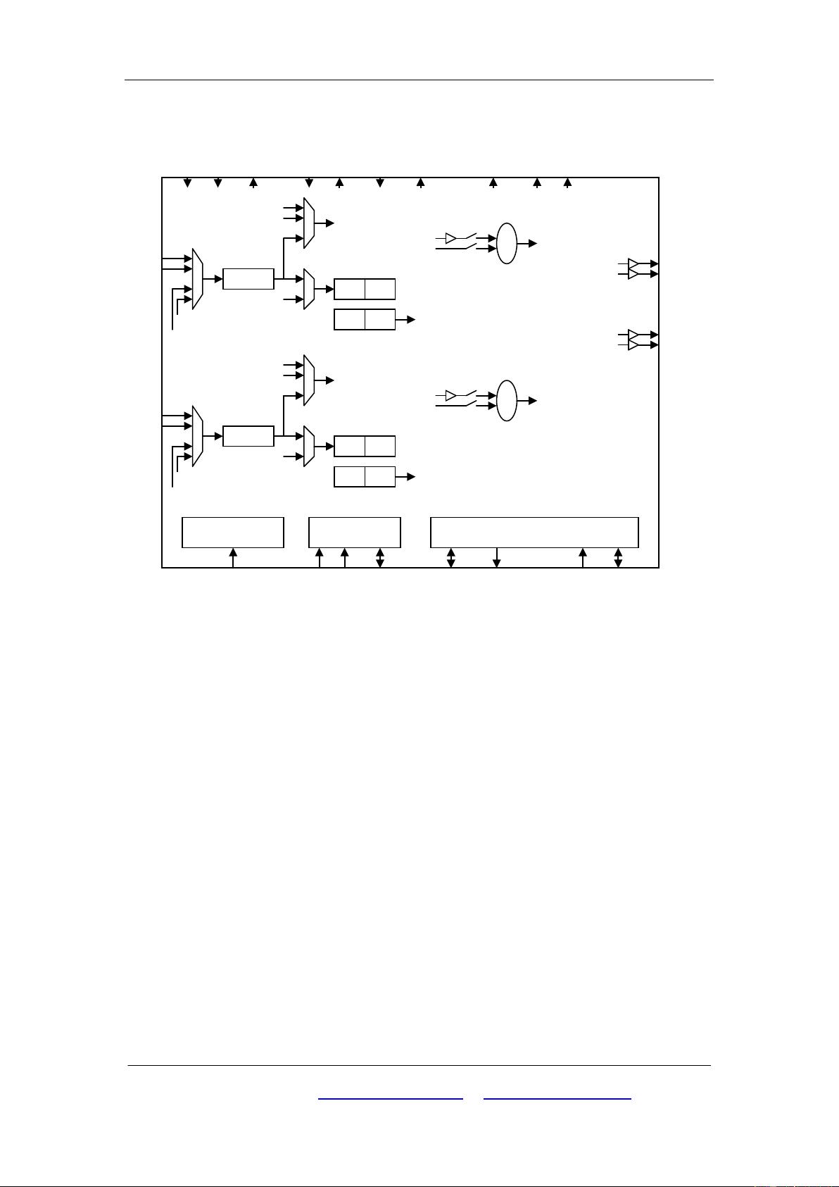
1 BLOCK DIAGRAM ............................................................................................................. 4
2 28-PIN QFN AND PIN DESCRIPTIONS ............................................................................ 5
3 TYPICAL APPLICATION CIRCUIT .................................................................................... 7
4 CLOCK MODES AND SAMPLING FREQUENCIES ......................................................... 7
5 MICRO-CONTROLLER CONFIGURATION INTERFACE ................................................. 9
5.1 SPI ..................................................................................................................................... 9
5.2 2-wire .............................................................................................................................. 10
6 CONFIGURATION REGISTER DEFINITION ................................................................... 11
6.1 Chip Control and Power Management ............................................................................ 13
6.1.1 Register 0 – Chip Control 1, Default 0000 0110 .............................................. 13
6.1.2 Register 1 – Chip Control 2, Default 0101 1100 .............................................. 13
6.1.3 Register 2 – Chip Power Management, Default 1100 0011 ........................... 14
6.1.4 Register 3 – ADC Power Management, Default 1111 1100 ............................ 14
6.1.5 Register 4 – DAC Power Management, Default 1100 0000........................... 15
6.1.6 Register 5 – Chip Low Power 1, Default 0000 0000 ....................................... 15
6.1.7 Register 6 – Chip Low Power 2, Default 0000 0000 ....................................... 15
6.1.8 Register 7 – Analog Voltage Management, Default 0111 1100 ..................... 15
6.1.9 Register 8 – Master Mode Control, Default 1000 0000 .................................. 16
6.2 ADC Control ................................................................................................................... 16
6.2.1 Register 9 – ADC Control 1, Default 0000 0000 .............................................. 16
6.2.2 Register 10 – ADC Control 2, Default 0000 0000 ............................................ 17
6.2.3 Register 11 – ADC Control 3, Default 0000 0010 ............................................ 17
6.2.4 Register 12 – ADC Control 4, Default 0000 0000 ............................................ 18
6.2.5 Register 13 – ADC Control 5, Default 0000 0110 ............................................ 18
6.2.6 Register 14 – ADC Control 6, Default 0011 0000 ............................................ 19
6.2.7 Register 15 – ADC Control 7, Default 0010 0000 ............................................ 19
6.2.8 Register 16 – ADC Control 8, Default 1100 0000 ............................................ 19
6.2.9 Register 17 – ADC Control 9, Default 1100 0000 ............................................ 20
6.2.10 Register 18 – ADC Control 10, Default 0011 1000 .......................................... 20
6.2.11 Register 19 – ADC Control 11, Default 1011 0000 .......................................... 20
6.2.12 Register 20 – ADC Control 12, Default 0011 0010 .......................................... 21
6.2.13 Register 21 – ADC Control 13, Default 0000 0110 .......................................... 22
6.2.14 Register 22 – ADC Control 14, Default 0000 0000 ......................................... 22
6.3 DAC Control ................................................................................................................... 22
6.3.1 Register 23 – DAC Control 1, Default 0000 0000 ........................................... 22
6.3.2 Register 24 – DAC Control 2, Default 0000 0110 ............................................ 23
6.3.3 Register 25 – DAC Control 3, Default 0010 0010 ........................................... 23
6.3.4 Register 26 – DAC Control 4, Default 1100 0000 ............................................ 24
6.3.5 Register 27 – DAC Control 5, Default 1100 0000 ............................................ 24
6.3.6 Register 28 – DAC Control 6, Default 0000 1000 ........................................... 24
6.3.7 Register 29 – DAC Control 7, Default 0000 0000 ........................................... 24
6.3.8 Register 30 – DAC Control 8, Default 0001 1111 ............................................ 25
6.3.9 Register 31 – DAC Control 9, Default 1111 0111 ............................................. 25
Everest Semiconductor ES8388
Revision 12.0 November 2023
Latest datasheet: www.everest-semi.com
or info@everest-semi.com
3
6.3.10 Register 32 – DAC Control 10, Default 1111 1101 .......................................... 25
6.3.11 Register 33 – DAC Control 11, Default 1111 1111 ........................................... 25
6.3.12 Register 34 – DAC Control 12, Default 0001 1111 .......................................... 25
6.3.13 Register 35 – DAC Control 13, Default 1111 0111 ........................................... 25
6.3.14 Register 36 – DAC Control 14, Default 1111 1101 .......................................... 25
6.3.15 Register 37 – DAC Control 15, Default 1111 1111 ........................................... 26
6.3.16 Register 38 – DAC Control 16, Default 0000 0000 ......................................... 26
6.3.17 Register 39 – DAC Control 17, Default 0011 1000 .......................................... 26
6.3.18 Register 40 – DAC Control 18, Default 0010 1000 ......................................... 26
6.3.19 Register 41 – DAC Control 19, Default 0010 1000 ......................................... 26
6.3.20 Register 42 – DAC Control 20, Default 0011 1000 .......................................... 27
6.3.21 Register 43 – DAC Control 21, Default 0000 0000 ......................................... 27
6.3.22 Register 44 – DAC Control 22, Default 0000 0000 ......................................... 27
6.3.23 Register 45 – DAC Control 23, Default 0000 0000 ......................................... 27
6.3.24 Register 46 – DAC Control 24, Default 0000 0000 ......................................... 27
6.3.25 Register 47 – DAC Control 25, Default 0000 0000 ......................................... 28
6.3.26 Register 48 – DAC Control 26, Default 0000 0000 ......................................... 28
6.3.27 Register 49 – DAC Control 27, Default 0000 0000 ......................................... 28
6.3.28 Register 50 – DAC Control 28, Default 0000 0000 ......................................... 29
6.3.29 Register 51 – DAC Control 29, Default 1010 1010 ......................................... 29
6.3.30 Register 52 – DAC Control 30, Default 1010 1010 ......................................... 29
7 Digital Audio Interface ...................................................................................................... 29
8 ELECTRICAL CHARACTERISTICS ................................................................................ 30
8.1 Absolute Maximum Ratings ........................................................................................... 30
8.2 Recommended Operating Conditions ............................................................................. 31
8.3 ADC Analog and Filter Characteristics and Specifications ............................................ 31
8.4 DAC Analog and Filter Characteristics and Specifications ............................................ 32
8.5 Power Consumption Characteristics ............................................................................... 32
8.6 Serial Audio Port Switching Specifications .................................................................... 33
8.7 Serial Control Port Switching Specifications .................................................................. 34
9 PACKAGE INFORMATION (UNIT: MM) .......................................................................... 35
10 CORPOARATION INFORMATION .............................................................................. 36
11 IMPORTANT NOTICE AND DISCLAIMER .................................................................. 36
Everest Semiconductor ES8388
Revision 12.0 November 2023
Latest datasheet: www.everest-semi.com
or info@everest-semi.com
4
1 BLOCK DIAGRAM
mic amp
ADC
mux
ALC
LIN
mux
LIN1
micL
micL+micR
LIN2
SE DAC DACL
mic amp
ADC
mux
ALC
RIN
mux
RIN1
micR
micL+micR
SE DAC DACR
mixL
+
LIN
DACL
mixR
+
RIN
DACR
mixL
mixR
LOUT1
ROUT1
mixL
mixR
LOUT2
ROUT2
DVDD PVDD DGND AVDD AGND HPVDD HPGND ADCVREF VREF VMID
MCLK
Clock Manager uC Interface
CE CCLK CDATA
Serial Audio Data
LRCK ASDOUT DSDIN SCLK
mux
RIN1
RIN2
LIN1-RIN1
LIN2-RIN2
mux
LIN1
LIN2
LIN1-RIN1
LIN2-RIN2
RIN2
Everest Semiconductor ES8388
Revision 12.0 November 2023
Latest datasheet: www.everest-semi.com
or info@everest-semi.com
5
2 28-PIN QFN AND PIN DESCRIPTIONS
CCLK
CDATA
CE
NC
LIN1
RIN1
LIN2
RIN2
VMID
ADCVREF
AGND
AVDD
HPVDD
LOUT2
ASDOUT
NC
VREF
ROUT1
LOUT1
HPGND
ROUT2
MCLK
DVDD
PVDD
DGND
SCLK
DSDIN
LRCK
8
9
10
11
12
13
14
21
20
19
18
17
16
15
28
27
26
25
24
23
22
1
2
3
4
5
6
7
剩余35页未读,继续阅读
资源评论
MIPSA
- 粉丝: 64
- 资源: 6
上传资源 快速赚钱
- 我的内容管理 展开
- 我的资源 快来上传第一个资源
- 我的收益 登录查看自己的收益
- 我的积分 登录查看自己的积分
- 我的C币 登录后查看C币余额
- 我的收藏
- 我的下载
- 下载帮助
安全验证
文档复制为VIP权益,开通VIP直接复制
信息提交成功