
UM10326_1 © NXP B.V. 2009. All rights reserved.
User manual Rev. 1 — 18 February 2009 5 of 723
NXP Semiconductors
UM10326
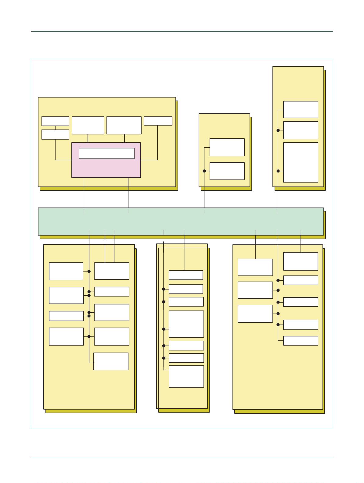
Chapter 1: LPC32x0 Introductory information
2. Features
• ARM926EJS processor, running at CPU clock speeds up to 266 MHz
• A Vector Floating Point coprocessor.
• A 32 KB instruction cache and a 32 KB data cache.
• Up to 256 KB of internal SRAM.
• Selectable boot-up from various external devices: NAND Flash, SPI memory, USB,
UART, or static memory.
• A Multi-layer AHB system that provides a separate bus for each AHB master,
including both an instruction and data bus for the CPU, two data busses for the DMA
controller, and another bus for the USB controller, one for the LCD and a final one for
the Ethernet MAC. There are no arbitration delays in the system unless two masters
attempt to access the same slave at the same time.
• An External memory controller for DDR and SDR SDRAM, as well as static devices.
– The address bus provides up to 16 MB for each of the 4 static chip selects.
– The controller provides two dynamic memory chip selects addressing up to
512 MB each.
• Two NAND Flash controllers. One for single level NAND Flash devices and the other
for multi-level NAND Flash devices.
• An Interrupt Controller, supporting 73 interrupt sources.
• An eight channel General Purpose AHB DMA controller (GPDMA) that can be used
with the SD card port, the 14-clock UARTs, I2S ports, and SPI interfaces, as well as
memory-to-memory transfers.
• Serial Interfaces:
– A 10/100 Ethernet MAC with dedicated DMA Controller.
– A USB interface supporting either Device, Host (OHCI compliant), or On-The-Go
(OTG) with an integral DMA controller and dedicated PLL to generate the required
48 MHz USB clock.
– Four standard UARTs with fractional baud rate generation and 64 byte FIFOs. One
of the standard UART’s supports IrDA.
– Three additional 14-clock UARTs intended for on-board communications that
support baudrates up to 921,600 bps when using a 13 MHz main oscillator.All
14-clock UARTs provide 64-byte FIFOs
– Two SPI controllers.
– Two SSP controllers
– Two I2C-bus Interfaces with standard open drain pins. The I2C-bus Interfaces
support single master, slave and multi-master I2C configurations.
– Two I2S interfaces, each with separate input and output channels. Each channel
can be operated independently on 3 pins, or both input and output with one I2S
interface can be done on only 4 pins.
• Additional Peripherals:
– LCD controller supporting both STN and TFT panels, with dedicated DMA
controller. Programmable display resolution up to 1024x768.
– Secure Digital (SD) memory card interface.


 wuhaiyunyiyi2012-11-20是2008年的,下载的时候注意下
 奈斯吆西2012-12-29还行 标准的资料
 robincsu2012-05-22不错,找了好久才找到,是官方的用户手册


