Mosfet 基础 Mosfet 基础

需积分: 0 111 浏览量
更新于2009-05-15
收藏 363KB PDF 举报
### MOSFET基础知识
#### 一、MOSFET历史
MOSFET(金属氧化物半导体场效应晶体管)的概念早在20世纪20年代至30年代就已经被提出,这比双极型晶体管(BJT)的发明早了大约20年。当时,美国科学家J.E. Lilienfeld提出了一个具有两个金属触点并在半导体顶部放置一块金属板(如铝)的晶体管模型。通过在金属板上施加电压,在半导体表面形成电场,从而实现对触点间电流的控制。
#### 二、场效应晶体管(FET)
**1. JFET(结型场效应晶体管)**
- **定义**:JFET是一种利用外加电压产生的电场来控制载流子(电子或空穴)流动的器件。
- **工作原理**:通过改变栅极电压来控制耗尽区的宽度,进而影响沟道电阻,实现对电流的控制。
- **特性**:JFET适用于高频和低噪声应用。
**2. MOSFET(金属氧化物半导体场效应晶体管)**
- **定义**:MOSFET是一种利用栅极电压控制半导体沟道中的载流子浓度,从而控制源极与漏极端之间的电流的晶体管。
- **工作原理**:通过在栅极与半导体之间施加电压,改变半导体沟道区域的导电性能。
- **应用**:广泛应用于电源开关、放大器、数字逻辑电路等领域。
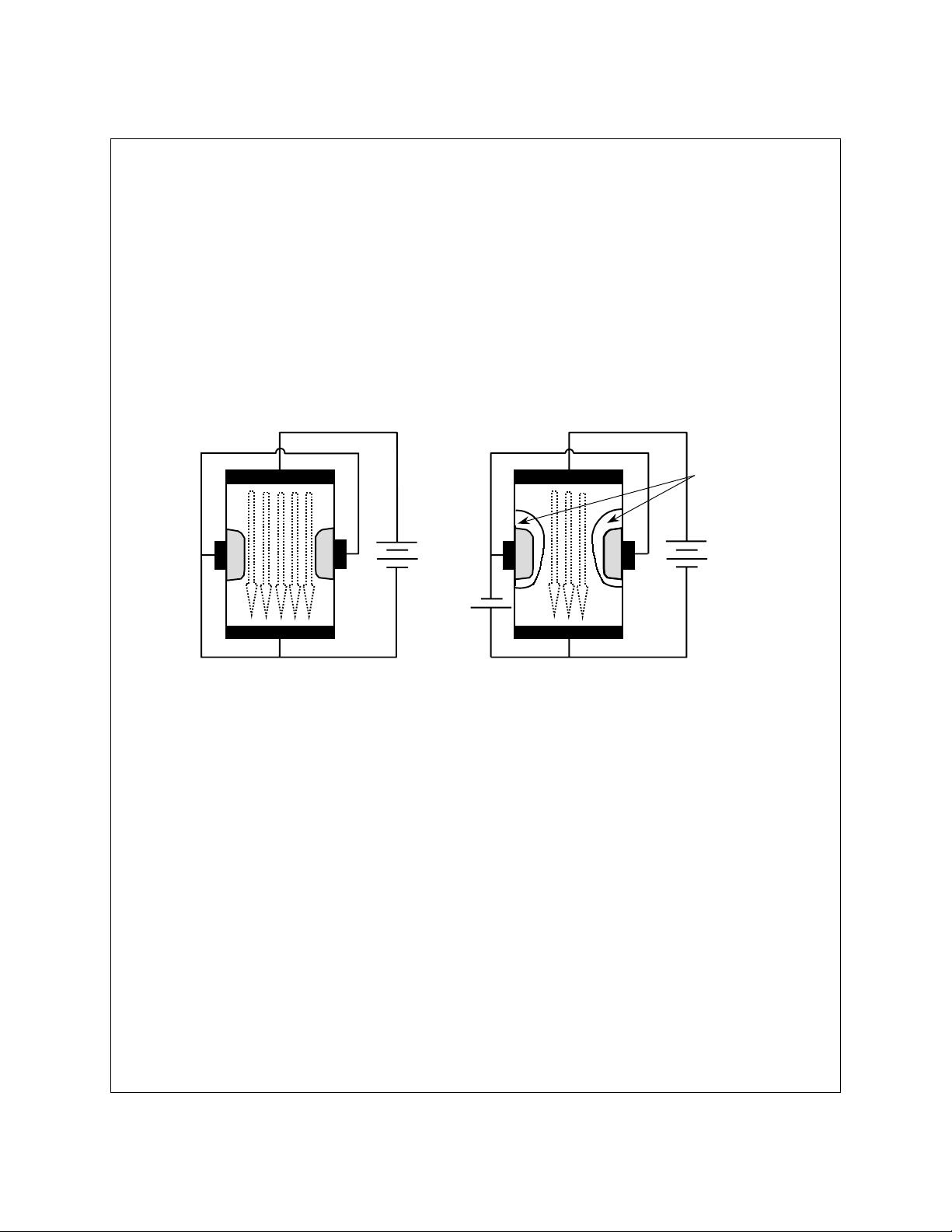
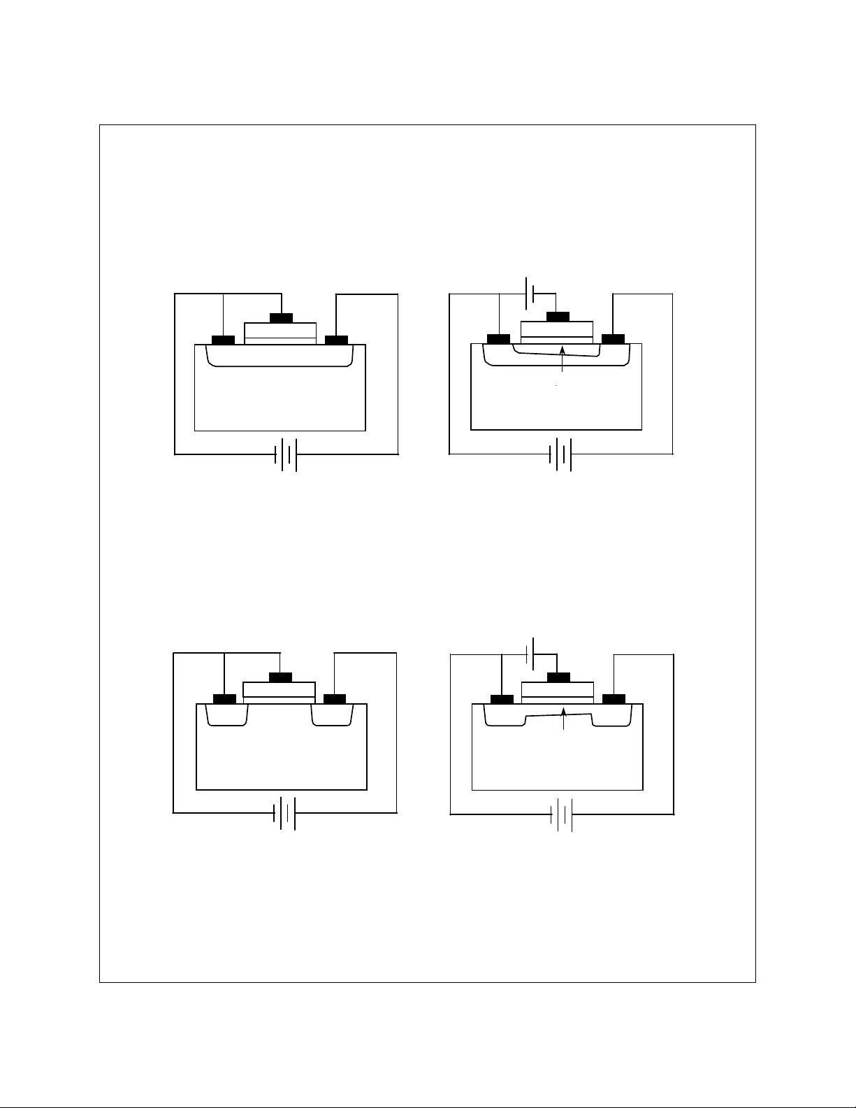
#### 三、MOSFET结构
**1. 横向通道结构**
- 在这种结构中,源极、栅极、漏极排列在同一平面上。
- 适用于集成电路中的小尺寸MOSFET。
**2. 垂直通道结构**
- 源极和漏极位于垂直方向上,栅极围绕着源极和漏极之间的通道。
- 这种结构可以提高MOSFET的击穿电压,适用于高压应用。
#### 四、MOSFET特性
**1. 优点**
- **高输入阻抗**:由于栅极与沟道之间有绝缘层隔离,使得栅极的输入阻抗非常高。
- **快速开关**:MOSFET的开关速度非常快,适用于高频应用。
- **低导通损耗**:在导通状态下,MOSFET的电阻较低,从而减少了导通时的功率损耗。
- **易于集成**:易于与其他CMOS电路集成。
**2. 缺点**
- **热稳定性**:相比其他类型的晶体管,MOSFET的热稳定性较差。
- **栅极击穿风险**:栅极电压过高可能导致栅极绝缘层击穿。
**3. 基本特性**
- **转移特性**:表示栅极电压与漏极电流之间的关系。
- **输出特性**:表示漏极电压与漏极电流之间的关系。
#### 五、MOSFET开关状态
**1. 关断状态**
- 当栅极电压低于阈值电压时,MOSFET处于关断状态,几乎无电流通过。
**2. 开通瞬态**
- 在开通瞬间,栅极电压迅速上升超过阈值电压,导致MOSFET进入过渡状态。
- 这个过程中可能会产生一定的能量损失。
**3. 导通状态**
- 在此状态下,MOSFET完全导通,漏极与源极之间的电阻非常小。
- 此时主要关注的是导通电阻,它决定了导通状态下的功耗。
**4. 关断瞬态**
- 关闭过程中,栅极电压下降,MOSFET逐渐进入关断状态。
- 这个过程同样会产生能量损失。
#### 六、MOSFET用户手册
**1. 电容特性**
- MOSFET内部存在三种电容:栅极-源极电容、栅极-漏极电容以及源极-漏极电容。
- 这些电容会影响MOSFET的开关速度。
**2. 栅极电荷特性**
- 栅极电荷是指当MOSFET从关断状态切换到导通状态时,栅极所积累的电荷量。
- 栅极电荷是评估MOSFET开关性能的一个重要参数。
**3. 漏-源极导通电阻**
- 导通电阻是衡量MOSFET导通状态下漏极与源极之间电阻的参数。
- 该参数直接影响MOSFET在导通状态下的功耗。
**4. 阈值电压**
- 阈值电压是使MOSFET从关断状态转变为导通状态所需的最小栅极电压。
- 对于MOSFET的设计和选择至关重要。
**5. 跨导**
- 跨导反映了栅极电压变化引起漏极电流变化的程度,是MOSFET增益的一种度量。
**6. 漏-源极击穿电压**
- 击穿电压是MOSFET所能承受的最大漏-源极电压。
- 超过此电压会导致MOSFET损坏。
**7. 漏-源极泄漏电流**
- 在关断状态下,漏极与源极之间会有一小部分泄漏电流。
- 泄漏电流通常很小,但在某些应用中可能需要考虑。
**8. 栅-源极电压**
- 栅-源极电压是控制MOSFET导通状态的关键参数。
- 它直接影响MOSFET的工作状态。
**9. 栅-源极泄漏电流**
- 即使在没有外部偏置的情况下,栅极与源极之间也会存在微小的泄漏电流。
- 在某些精密应用中,需要对此进行精确控制。
**10. 开关特性**
- 包括开通时间和关断时间等。
- 这些特性对于高速开关应用非常重要。
**11. 单脉冲雪崩能量**
- MOSFET在短时间内能够承受的最大能量。
- 这是衡量MOSFET耐受瞬态过载能力的一个指标。
**12. 重复性雪崩评级**
- 表示MOSFET能够重复承受的最大雪崩能量。
- 用于评估MOSFET在反复受到过载冲击时的可靠性。
**13. 漏-源极dv/dt评级**
- 表示MOSFET能够承受的最大电压变化率。
- 对于高速开关应用尤为重要。
**14. 热特性**
- 包括最大结温、热阻等。
- 热特性对于确保MOSFET在各种温度条件下的可靠运行至关重要。
**15. 连续漏极电流**
- 指MOSFET在正常工作条件下能够连续承载的最大电流。
- 是设计电路时的重要参考数据。
**16. 总功耗**
- 包括导通状态功耗、开关状态功耗等。
- 在计算MOSFET散热需求时非常关键。
**17. 安全工作区**
- 定义了MOSFET在不同工作条件下的安全工作范围。
- 超出安全工作区可能会导致MOSFET损坏。
#### PWM计算
MOSFET在许多应用中都与PWM技术密切相关。通过调整PWM信号的占空比,可以控制MOSFET的导通时间,进而调节输出功率。在计算PWM相关的MOSFET参数时,需要考虑以下几个方面:
1. **开关频率**:即PWM信号的频率,决定了MOSFET每秒开关次数。
2. **占空比**:决定了MOSFET导通时间与整个周期时间的比例。
3. **开关损耗**:包括开通损耗和关断损耗,需要根据MOSFET的开关特性和PWM信号的频率进行计算。
4. **导通损耗**:由MOSFET的导通电阻决定,与PWM信号的占空比有关。
MOSFET作为现代电力电子领域中不可或缺的一部分,其特性、工作原理及应用等方面的知识对于工程师来说十分重要。掌握这些基础理论不仅有助于理解MOSFET的基本工作方式,还能为设计高性能电力电子设备提供必要的技术支持。

Rev D, July 2000
July, 2000
1
AN9010
MOSFET Basics
By K.S.Oh
CONTENTS
1. History of Power MOSFETs........................................................................................................ 2
2. FETs ........................................................................................................................................... 3
1) JFET....................................................................................................................................... 3
2) MOSFET ................................................................................................................................ 4
3. The structure of MOSFET .......................................................................................................... 5
1) Lateral Channel Structure ..................................................................................................... 5
2) Vertical Channel Structure ..................................................................................................... 5
4. The characteristics of MOSFET .................................................................................................7
1) Advantages ............................................................................................................................ 7
2) Disadvantage ......................................................................................................................... 7
3) Basic Characteristics.............................................................................................................. 7
5. Characteristics of MOSFET’s ON, OFF.................................................................................... 10
1) Off State ............................................................................................................................... 10
2) Turn – on Transient ...............................................................................................................11
3) On State............................................................................................................................... 13
4) Turn – off Transient .............................................................................................................. 14
6. User’s Manual .......................................................................................................................... 14
1) Characteristics of Capacitance ............................................................................................ 14
2) Characteristics of the Gate Charge...................................................................................... 17
3) Drain – source On Resistance ............................................................................................. 20
4) Threshold Voltage ................................................................................................................ 22
5) Transconductance................................................................................................................ 22
6) Drain – source Breakdown Voltage
Breakdown Voltage Temp. Coeff. ......................................................................................... 23
7) Drain – to – source Leakage Current ................................................................................... 24
8) Gate – to – source Voltage...................................................................................................24
9) Gate – source Leakage, Forward / Reverse ........................................................................ 24
10) Switching Characteristics ...................................................................................................24
11) Single – pulsed Avalanche Energy..................................................................................... 25
12) Repetitive Avalanche Rating .............................................................................................. 27
13) Drain – to – source dv / dt Ratings..................................................................................... 27
14) Thermal Characteristics .....................................................................................................32
15) Continuous Drain Current, Drain Current – pulsed ............................................................ 35
16) Total Power Dissipation, Linear Derating Factor ................................................................ 35
17) Safe Operating Areas......................................................................................................... 36


剩余36页未读,继续阅读
2011-04-16 上传
171 浏览量
153 浏览量
126 浏览量
2010-02-03 上传
2011-08-12 上传
120 浏览量
2020-07-29 上传
171 浏览量
136 浏览量
199 浏览量
152 浏览量
173 浏览量
2021-12-27 上传
169 浏览量
110 浏览量
2021-10-30 上传
101 浏览量
2008-06-17 上传
资源评论


lucky_xhq
- 粉丝: 0
- 资源: 4


最新资源
- 基于PLC的全自动洗衣机控制系统设计:硬件与软件的完美结合方案,基于PLC的全自动洗衣机控制系统设计详解含硬件和软件设计章节一套完整方案,基于PLC全自动洗衣机控制系统设计 含Word文档一整套 前
- 基于COMSOL的结晶凝固过程仿真:考虑温度场、浓度场、相变及物质偏析的全方位分析,COMSOL仿真模拟结晶过程:涵盖温度场、浓度场、相变及物质偏析等多元因素研究,comsol 仿真结晶,凝固,考虑温
- stm32 OLED显示模块 寄存器方式代码
- 基于Matlab的迁移学习技术用于滚动轴承故障诊断,振动信号转图像处理并高精度分类,基于Matlab的迁移学习滚动轴承故障诊断系统:高准确率,简易操作,Matlab 基于迁移学习的滚动轴承故障诊断 1
- 双缸水平蒸汽机3D 双缸水平蒸汽机
- 基于XAFS数据处理的拟合算法及小波变换应用研究,基于XAFS数据处理的拟合算法及小波变换应用研究,xafs数据处理,拟合,小波变 ,xafs数据处理; 拟合; 小波变换,Xafs数据处理与拟合的小波
- 无线通信Mimo系统中STBC空时编码与MRC最大比合并的性能比较研究(基于Matlab 2016b版本),无线通信MIMO系统中的STBC空时编码与MRC最大比合并技术性能研究,基于Matlab 2
- 基于Python的Django-vue基于Spark的国漫推荐系统实现源码-说明文档-演示视频.zip
- C#实现多协议数据传输:OPC与DCS无DCOM配置读取及高效数据转发方案,C#实现无需DCOM配置的OPC与DCS数据传输:通过Socket转发至其他电脑或MODBUS/UDP协议实现高效数据读取与
- C语言基础入门学习笔记大纲.pdf
- 回溯组合问题_202503061306_54460.hinote
- 火狐判断安装_64位版本 (1).exe
- 基于python+PYQT开发的电子发票管理软件(源码+说明)
- 基于STM32F103C8T6与ATT7022芯片的三相交流电测量RTU-功能丰富、数据准确、稳定可靠的电能监控系统,基于STM32与ATT7022芯片的三相交流电测量RTU系统:集成电压、电流及多
- 回溯组合问题_202503061309_56587.pdf
- 基于python和豆包开发的根据提示词生成脚本 通过视频脚本调用微软tts生成语音功能的软件(源码)
