没有合适的资源?快使用搜索试试~ 我知道了~
IS61WV51216ALL.pdf
需积分: 14 8 下载量 117 浏览量
2010-09-04
23:04:30
上传
评论
收藏 205KB PDF 举报
温馨提示
试读
20页
该文档介绍了IS61WV51216ALL的详细资料,为存储器编程提供了极大的便利
资源推荐
资源详情
资源评论
Integrated Silicon Solution, Inc. — www.issi.com
1
Rev. F
10/01/09
Copyright © 2006 Integrated Silicon Solution, Inc. All rights reserved. ISSI reserves the right to make changes to this specification and its products at any time
without notice. ISSI assumes no liability arising out of the application or use of any information, products or services described herein. Customers are advised to
obtain the latest version of this device specification before relying on any published information and before placing orders for products.
IS61WV51216ALL
IS61WV51216BLL
IS64WV51216BLL
512K x 16 HIGH-SPEED ASYNCHRONOUS
CMOS STATIC RAM WITH 3.3V SUPPLY
OCTOBER 2009
FEATURES
• High-speed access times:
8, 10, 20 ns
• High-performance, low-power CMOS process
• Multiple center power and ground pins for greater
noise immunity
• Easy memory expansion with CE and OE op-
tions
• CE power-down
• Fully static operation: no clock or refresh
required
• TTL compatible inputs and outputs
• Single power supply
V
DD 1.65V to 2.2V (IS61WV51216ALL)
speed = 20ns for V
DD 1.65V to 2.2V
V
DD 2.4V to 3.6V (IS61/64WV51216BLL)
speed = 10ns for V
DD 2.4V to 3.6V
speed = 8ns for V
DD 3.3V + 5%
• Packages available:
–
48-ball miniBGA (9mm x 11mm)
– 44-pin TSOP (Type II)
• Industrial and Automotive Temperature Support
• Lead-free available
• Data control for upper and lower bytes
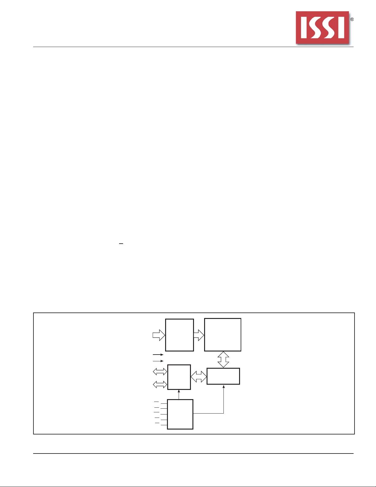
FUNCTIONAL BLOCK DIAGRAM
DESCRIPTION
The ISSI IS61WV51216ALL/BLL and IS64WV51216BLL
are high-speed, 8M-bit static RAMs organized as 512K
words by 16 bits. It is fabricated using ISSI's high-perform-
ance CMOS technology. This highly reliable process coupled
with innovative circuit design techniques, yields high-perfor-
mance and low power consumption devices.
When CE is HIGH (deselected), the device assumes a
standby mode at which the power dissipation can be
reduced down with CMOS input levels.
Easy memory expansion is provided by using Chip Enable
and Output Enable inputs, CE and OE. The active LOW
Write Enable (WE) controls both writing and reading of the
memory. A data byte allows Upper Byte (UB) and Lower
Byte (LB) access.
The device is packaged in the JEDEC standard 44-pin
TSOP Type II and 48-pin Mini BGA (9mm x 11mm).
A0-A18
CE
OE
WE
512K x 16
MEMORY ARRAY
DECODER
COLUMN I/O
CONTROL
CIRCUIT
GND
VDD
I/O
DATA
CIRCUIT
I/O0-I/O7
Lower Byte
I/O8-I/O15
Upper Byte
UB
LB
2
Integrated Silicon Solution, Inc. — www.issi.com
Rev. F
10/01/09
IS61WV51216ALL
IS61WV51216BLL
IS64WV51216BLL
PIN DESCRIPTIONS
A0-A18 Address Inputs
I/O0-I/O15 Data Inputs/Outputs
CE Chip Enable Input
OE Output Enable Input
WE Write Enable Input
LB Lower-byte Control (I/O0-I/O7)
UB Upper-byte Control (I/O8-I/O15)
NC No Connection
VDD Power
GND Ground
48-pin mini BGA (9mmx11mm)
1 2 3 4 5 6
A
B
C
D
E
F
G
H
LB
OE
A0
A1
A2
NC
I/O
8
UB A3
A4
CE I/O
0
I/O
9
I/O
10
A5
A6
I/O
1
I/O
2
GND
I/O
11
A17
A7
I/O
3
VDD
VDD
I/O
12
NC
A16
I/O
4
GND
I/O
14
I/O
13
A14
A15
I/O
5
I/O
6
I/O
15
NC
A12
A13
WE
I/O
7
A18
A8
A9
A10
A11 NC
Integrated Silicon Solution, Inc. — www.issi.com
3
Rev. F
10/01/09
IS61WV51216ALL
IS61WV51216BLL
IS64WV51216BLL
PIN DESCRIPTIONS
A0-A18 Address Inputs
I/O0-I/O15 Data Inputs/Outputs
CE Chip Enable Input
OE Output Enable Input
WE Write Enable Input
LB Lower-byte Control (I/O0-I/O7)
UB Upper-byte Control (I/O8-I/O15)
NC No Connection
VDD Power
GND Ground
44-Pin TSOP (Type II)
1
2
3
4
5
6
7
8
9
10
11
12
13
14
15
16
17
18
19
20
21
22
44
43
42
41
40
39
38
37
36
35
34
33
32
31
30
29
28
27
26
25
24
23
A0
A1
A2
A3
A4
CE
I/O0
I/O1
I/O2
I/O3
VDD
GND
I/O4
I/O5
I/O6
I/O7
WE
A5
A6
A7
A8
A9
A17
A16
A15
OE
UB
LB
I/O15
I/O14
I/O13
I/O12
GND
VDD
I/O11
I/O10
I/O9
I/O8
A18
A14
A13
A12
A11
A10
PIN CONFIGURATIONS
4
Integrated Silicon Solution, Inc. — www.issi.com
Rev. F
10/01/09
IS61WV51216ALL
IS61WV51216BLL
IS64WV51216BLL
ABSOLUTE MAXIMUM RATINGS
(1)
Symbol Parameter Value Unit
VTERM Terminal Voltage with Respect to GND –0.5 to VDD + 0.5 V
VDD VDD Relates to GND –0.3 to 4.0 V
TSTG Storage Temperature –65 to +150 °C
PT Power Dissipation 1.0 W
Notes:
1. Stress greater than those listed under ABSOLUTE MAXIMUM RATINGS may cause permanent damage
to the device. This is a stress rating only and functional operation of the device at these or any other
conditions above those indicated in the operational sections of this specification is not implied. Exposure
to absolute maximum rating conditions for extended periods may affect reliability.
CAPACITANCE
(1,2)
Symbol Parameter Conditions Max. Unit
CIN Input Capacitance VIN = 0V 6 pF
CI/O Input/Output Capacitance VOUT = 0V 8 pF
Notes:
1. Tested initially and after any design or process changes that may affect these parameters.
2. Test conditions: T
A = 25°C, f = 1 MHz, VDD = 3.3V.
TRUTH TABLE
I/O PIN
Mode
WEWE
WEWE
WE
CECE
CECE
CE
OEOE
OEOE
OE
LBLB
LBLB
LB
UBUB
UBUB
UB I/O0-I/O7 I/O8-I/O15 VDD Current
Not Selected X H X X X High-Z High-Z ISB1, ISB2
Output Disabled H L H X X High-Z High-Z ICC
X L X H H High-Z High-Z
Read H L L L H DOUT High-Z ICC
H L L H L High-Z DOUT
HLLLL DOUT DOUT
Write L L X L H DIN High-Z ICC
L L X H L High-Z DIN
LLXLL DIN DIN
剩余19页未读,继续阅读
资源评论
liyuanqing202
- 粉丝: 2
- 资源: 4
上传资源 快速赚钱
- 我的内容管理 展开
- 我的资源 快来上传第一个资源
- 我的收益 登录查看自己的收益
- 我的积分 登录查看自己的积分
- 我的C币 登录后查看C币余额
- 我的收藏
- 我的下载
- 下载帮助
最新资源
- 基于python的机械设计实用计算器,可计算电动机,传动装置,V带轮,齿轮,轴,轴承的几何或者力,运动学参数数值+源码+开发文档
- 基于HTML +JavaScript的元旦倒计时代码.docx
- 【Unity资源免费分享】孩子益智小游戏unity 5x系列Baby Doll House Cleaning
- 【资源免费分享】集市游戏(uniyt案例)
- 数据整理结果 2023-12-7 192544 6.dta
- 5.22前端基础(2)
- 糖尿病风险因素分析数据
- matlab项目源码基于matlab的声源定位广义互相关算法的实现.zip
- 基于Go的Dory-Engine应用上云引擎命令行客户端设计源码
- dotnet-core-uninstall-1.7.521001 github上下载下来,从github下载不下来时,可以使用这
资源上传下载、课程学习等过程中有任何疑问或建议,欢迎提出宝贵意见哦~我们会及时处理!
点击此处反馈
安全验证
文档复制为VIP权益,开通VIP直接复制
信息提交成功