没有合适的资源?快使用搜索试试~ 我知道了~
碳化硅40mΩ,1200V,带Kevin Source功能.支持5KW至40KW功率.光伏逆变器,光伏储能,OBC,便携式储能,工业电源,交通轨道,固态变压器等等场合,都非常适应.
资源详情
资源评论
资源推荐
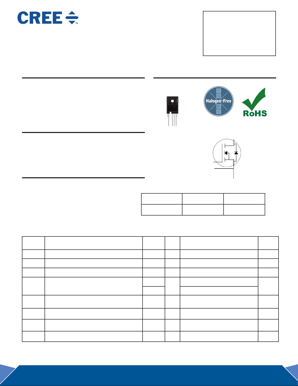
1 C3M0040120K Rev. 1, 10-2020
C3M0040120K
Silicon Carbide Power MOSFET
C3M
TM
MOSFET Technology
N-Channel Enhancement Mode
Features
• 3rd generation SiC MOSFET technology
• Optimized package with separate driver source pin
• 8mm of creepage distance between drain and source
• High blocking voltage with low on-resistance
• High-speed switching with low capacitances
• Fast intrinsic diode with low reverse recovery (Q
rr
)
• Halogen free, RoHS compliant
Benets
• Reduce switching losses and minimize gate ringing
• Higher system efciency
• Reduce cooling requirements
• Increase power density
• Increase system switching frequency
Applications
• Solar inverters
• EV motor drive
• High voltage DC/DC converters
• Switched mode power supplies
• Load switch
Package
Part Number Package
Marking
C3M0040120K TO 247-4 C3M0040120K
V
DS
1200 V
I
D
@
25˚C
66 A
R
DS(on)
40 mΩ
Maximum Ratings (T
C
= 25 ˚C unless otherwise specied)
Symbol Parameter Value Unit Test Conditions Note
V
DSmax
Drain - Source Voltage 1200 V V
GS
=
0 V, I
D
= 100 μA
V
GSmax
Gate - Source Voltage (dynamic) -8/+19 V AC (f >1 Hz) Note 1
V
GSop
Gate - Source Voltage (static) -4/+15 V Static Note 2
I
D
Continuous Drain Current
66
A
V
GS
= 15 V, T
C
= 25˚C
Fig. 19
48 V
GS
= 15 V, T
C
= 100˚C
I
D(pulse)
Pulsed Drain Current 100 A Pulse width t
P
limited by T
jmax
P
D
Power Dissipation 326 W T
C
=25˚C, T
J
= 175 ˚C Fig. 20
T
J
, T
stg
Operating Junction and Storage Temperature
-40 to
+175
˚C
T
L
Solder Temperature 260 ˚C 1.6mm (0.063”) from case for 10s
Note (1): When using MOSFET Body Diode V
GSmax
= -4V/+19V
Note (2): MOSFET can also safely operate at 0/+15 V
Drain
(Pin 1, TAB)
Power
Source
(Pin 2)
Driver
Source
(Pin 3)
Gate
(Pin 4)
Tab
Drain
1 2 3 4
D S S G
2 C3M0040120K Rev. 1, 10-2020
Electrical Characteristics (T
C
= 25˚C unless otherwise specied)
Symbol Parameter Min. Typ. Max. Unit Test Conditions Note
V
(BR)DSS
Drain-Source Breakdown Voltage 1200 V
V
GS
=
0 V, I
D
= 100 μA
V
GS(th)
Gate Threshold Voltage
1.8 2.7 3.6
V V
DS
= V
GS
, I
D
= 9.2 mA
Fig. 11
2.2
V V
DS
= V
GS
, I
D
= 9.2 mA, T
J
= 175ºC
I
DSS
Zero Gate Voltage Drain Current 1 50 μA
V
DS
= 1200 V, V
GS
= 0 V
I
GSS
Gate-Source Leakage Current 10 250 nA
V
GS
= 15 V, V
DS
= 0 V
R
DS(on)
Drain-Source On-State Resistance
40 53.5
mΩ
V
GS
= 15 V, I
D
= 33.3 A
Fig. 4,
5, 6
68
V
GS
= 15 V, I
D
= 33.3 A, T
J
= 175ºC
g
fs
Transconductance
21
S
V
DS
=
20 V, I
DS
=
33.3 A
Fig. 7
20
V
DS
=
20 V, I
DS
=
33.3 A, T
J
= 175ºC
C
iss
Input Capacitance 2900
pF
V
GS
= 0 V, V
DS
= 1000 V
f = 100 kHz
V
AC
= 25 mV
Fig. 17,
18
C
oss
Output Capacitance 103
C
rss
Reverse Transfer Capacitance 5
E
oss
C
oss
Stored Energy 60 μJ Fig. 16
E
ON
Turn-On Switching Energy (SiC Diode FWD) 243
μJ
V
DS
= 800 V, V
GS
= -4 V/+15 V,
I
D
= 33.3 A,
R
G(ext)
= 2.5Ω, L= 99 μH, Tj = 175ºC
Fig. 26
E
OFF
Turn Off Switching Energy (SiC Diode FWD) 104
E
ON
Turn-On Switching Energy (Body Diode FWD) 611
μJ
V
DS
= 800 V, V
GS
= -4 V/+15 V,
I
D
= 33.3 A,
R
G(ext)
= 2.5Ω, L= 99 μH, Tj = 175ºC
Fig. 26
E
OFF
Turn Off Switching Energy (Body Diode FWD) 99
t
d(on)
Turn-On Delay Time 13
ns
V
DD
= 800 V, V
GS
= -4 V/15 V
R
G(ext)
= 2.5 Ω, I
D
= 33.3 A, L= 99
Timing relative to V
DS
, Inductive load
Fig. 27
t
r
Rise Time 17
t
d(off)
Turn-Off Delay Time 23
t
f
Fall Time 9
R
G(int)
Internal Gate Resistance 3.5 Ω
f = 1 MHz
,
V
AC
=
25 mV
Q
gs
Gate to Source Charge 34
nC
V
DS
= 800 V, V
GS
= -4 V/15 V
I
D
= 33.3 A
Per IEC60747-8-4 pg 21
Fig. 12
Q
gd
Gate to Drain Charge 28
Q
g
Total Gate Charge 99
3 C3M0040120K Rev. 1, 10-2020
Reverse Diode Characteristics
(T
C
= 25˚C unless otherwise specied)
Symbol Parameter Typ. Max. Unit Test Conditions Note
V
SD
Diode Forward Voltage
5.5 V
V
GS
= -4 V, I
SD
= 20 A, T
J
= 25 °C
Fig. 8,
9, 10
4.9 V
V
GS
= -4 V, I
SD
= 20 A, T
J
= 175 °C
I
S
Continuous Diode Forward Current 51 A
V
GS
= -4 V, T
C
= 25˚C
Note 1
I
S, pulse
Diode pulse Current 100 A
V
GS
= -4 V, pulse width t
P
limited by T
jmax
Note 1
t
rr
Reverse Recover time 17 ns
V
GS
= -4 V, I
SD
= 33.3 A, V
R
= 800 V
dif/dt = 7725 A/µs, T
J
= 175 °C
Note 1Q
rr
Reverse Recovery Charge 850 nC
I
rrm
Peak Reverse Recovery Current 79 A
t
rr
Reverse Recover time 33 ns
V
GS
= -4 V, I
SD
= 33.3 A, V
R
= 800 V
dif/dt = 2325 A/µs, T
J
= 175 °C
Note 1Q
rr
Reverse Recovery Charge 691 nC
I
rrm
Peak Reverse Recovery Current 30 A
Thermal Characteristics
Symbol Parameter Typ. Unit Test Conditions Note
R
θJC
Thermal Resistance from Junction to Case 0.46
°C/W Fig. 21
R
θJA
Thermal Resistance From Junction to Ambient 40
剩余11页未读,继续阅读
lilang1314
- 粉丝: 1
- 资源: 11
上传资源 快速赚钱
- 我的内容管理 展开
- 我的资源 快来上传第一个资源
- 我的收益 登录查看自己的收益
- 我的积分 登录查看自己的积分
- 我的C币 登录后查看C币余额
- 我的收藏
- 我的下载
- 下载帮助
安全验证
文档复制为VIP权益,开通VIP直接复制
信息提交成功
评论0