没有合适的资源?快使用搜索试试~ 我知道了~
AT91SAM9260手册
4星 · 超过85%的资源 需积分: 10 9 下载量 141 浏览量
2013-04-08
19:25:15
上传
评论
收藏 8.29MB PDF 举报
温馨提示
试读
752页
AT91SAM9260用户手册英文版,包括arm内部资源的描述,以及寄存器等的说明
资源推荐
资源详情
资源评论
Features
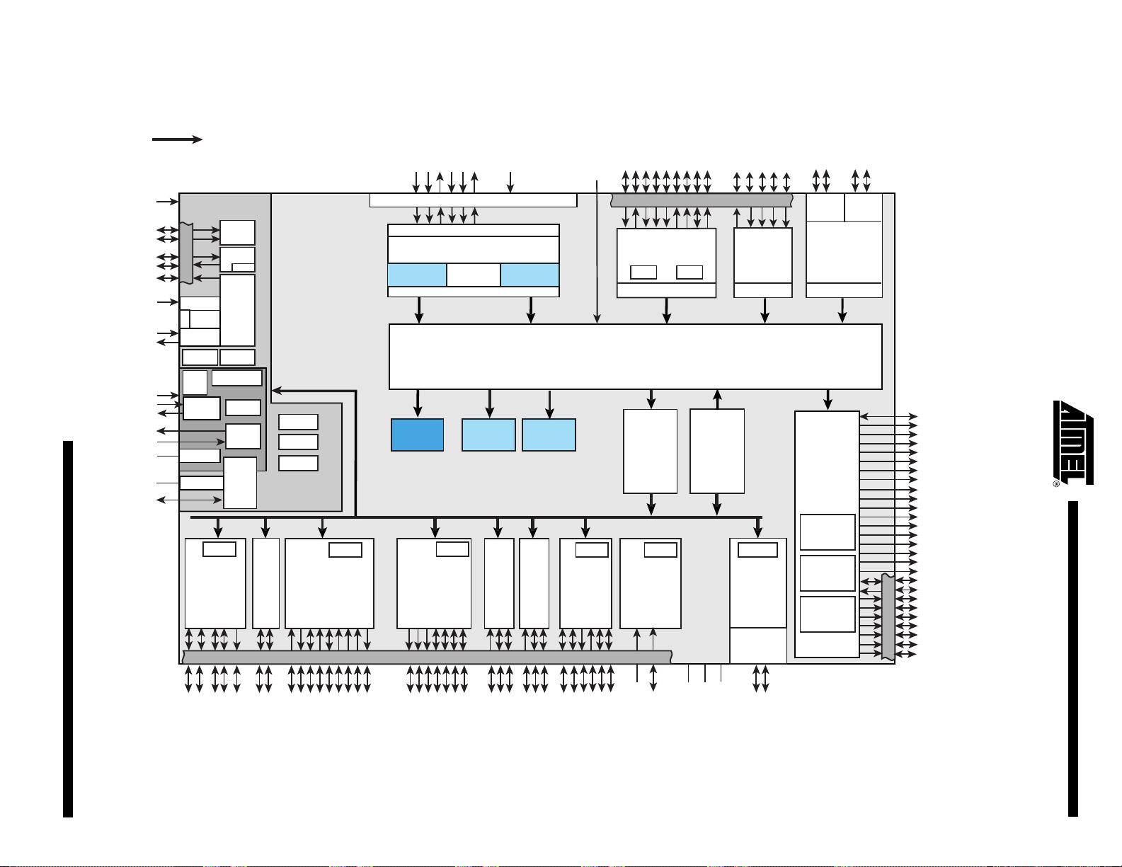
• Incorporates the ARM926EJ-S™ ARM
®
Thumb
®
Processor
– DSP Instruction Extensions, ARM Jazelle
®
Technology for Java
®
Acceleration
– 8-KByte Data Cache, 8-KByte Instruction Cache, Write Buffer
– 200 MIPS at 180 MHz
– Memory Management Unit
– EmbeddedICE
™
, Debug Communication Channel Support
• Additional Embedded Memories
– One 32-KByte Internal ROM, Single-cycle Access At Maximum Matrix Speed
– Two 4-KByte Internal SRAM, Single-cycle Access At Maximum Matrix Speed
• External Bus Interface (EBI)
– Supports SDRAM, Static Memory, ECC-enabled NAND Flash and CompactFlash
®
• USB 2.0 Full Speed (12 Mbits per second) Device Port
– On-chip Transceiver, 2,432-byte Configurable Integrated DPRAM
• USB 2.0 Full Speed (12 Mbits per second) Host Single Port in the 208-lead PQFP
Package and Double Port in 217-ball LFBGA Package
– Single or Dual On-chip Transceivers
– Integrated FIFOs and Dedicated DMA Channels
• Ethernet MAC 10/100 Base T
– Media Independent Interface or Reduced Media Independent Interface
– 28-byte FIFOs and Dedicated DMA Channels for Receive and Transmit
• Image Sensor Interface
– ITU-R BT. 601/656 External Interface, Programmable Frame Capture Rate
– 12-bit Data Interface for Support of High Sensibility Sensors
– SAV and EAV Synchronization, Preview Path with Scaler, YCbCr Format
• Bus Matrix
– Six 32-bit-layer Matrix
– Boot Mode Select Option, Remap Command
• Fully-featured System Controller, including
– Reset Controller, Shutdown Controller
– Four 32-bit Battery Backup Registers for a Total of 16 Bytes
– Clock Generator and Power Management Controller
– Advanced Interrupt Controller and Debug Unit
– Periodic Interval Timer, Watchdog Timer and Real-time Timer
• Reset Controller (RSTC)
– Based on a Power-on Reset Cell, Reset Source Identification and Reset Output
Control
• Clock Generator (CKGR)
– Selectable 32,768 Hz Low-power Oscillator or Internal Low Power RC Oscillator on
Battery Backup Power Supply, Providing a Permanent Slow Clock
– 3 to 20 MHz On-chip Oscillator, One up to 240 MHz PLL and One up to 130 MHz PLL
• Power Management Controller (PMC)
– Very Slow Clock Operating Mode, Software Programmable Power Optimization
Capabilities
– Two Programmable External Clock Signals
• Advanced Interrupt Controller (AIC)
– Individually Maskable, Eight-level Priority, Vectored Interrupt Sources
– Three External Interrupt Sources and One Fast Interrupt Source, Spurious
Interrupt Protected
6221B–ATARM–25-Jul-06
AT91 ARM
Thumb
Microcontrollers
AT91SAM9260
Preliminary
2
6221B–ATARM–25-Jul-06
AT91SAM9260 Preliminary
• Debug Unit (DBGU)
– 2-wire UART and Support for Debug Communication Channel, Programmable ICE Access Prevention
• Periodic Interval Timer (PIT)
– 20-bit Interval Timer plus 12-bit Interval Counter
• Watchdog Timer (WDT)
– Key-protected, Programmable Only Once, Windowed 16-bit Counter Running at Slow Clock
• Real-time Timer (RTT)
– 32-bit Free-running Backup Counter Running at Slow Clock with 16-bit Prescaler
• One 4-channel 10-bit Analog-to-Digital Converter
• Three 32-bit Parallel Input/Output Controllers (PIOA, PIOB, PIOC)
– 96 Programmable I/O Lines Multiplexed with up to Two Peripheral I/Os
– Input Change Interrupt Capability on Each I/O Line
– Individually Programmable Open-drain, Pull-up Resistor and Synchronous Output
– High-current Drive I/O Lines, Up to 16 mA Each
• Peripheral DMA Controller Channels (PDC)
• One Two-slot MultiMedia Card Interface (MCI)
– SDCard/SDIO and MultiMediaCard
™
Compliant
– Automatic Protocol Control and Fast Automatic Data Transfers with PDC
• One Synchronous Serial Controller (SSC)
– Independent Clock and Frame Sync Signals for Each Receiver and Transmitter
– I²S Analog Interface Support, Time Division Multiplex Support
– High-speed Continuous Data Stream Capabilities with 32-bit Data Transfer
• Four Universal Synchronous/Asynchronous Receiver Transmitters (USART)
– Individual Baud Rate Generator, IrDA
®
Infrared Modulation/Demodulation, Manchester Encoding/Decoding
– Support for ISO7816 T0/T1 Smart Card, Hardware Handshaking, RS485 Support
– Full Modem Signal Control on USART0
• Two 2-wire UARTs
• Two Master/Slave Serial Peripheral Interfaces (SPI)
– 8- to 16-bit Programmable Data Length, Four External Peripheral Chip Selects
– Synchronous Communications
• Two Three-channel 16-bit Timer/Counters (TC)
– Three External Clock Inputs, Two Multi-purpose I/O Pins per Channel
– Double PWM Generation, Capture/Waveform Mode, Up/Down Capability
– High-Drive Capability on Outputs TIOA0, TIOA1, TIOA2
• One Two-wire Interface (TWI)
– Master, Multi-master and Slave Mode Operation
– General Call Supported in Slave Mode
• IEEE
®
1149.1 JTAG Boundary Scan on All Digital Pins
• Required Power Supplies:
– 1.65V to 1.95V for VDDBU, VDDCORE, VDDOSC and VDDPLL
– 1.65V to 3.6V for VDDIOP1 (Peripheral I/Os)
– 3.0V to 3.6V for VDDIOP0 and VDDANA (Analog-to-digital Converter)
– Programmable 1.65V to 1.95V or 3.0V to 3.6V for VDDIOM (Memory I/Os)
• Available in a 208-lead PQFP Green and a 217-ball LFBGA RoHS-compliant Package
3
6221B–ATARM–25-Jul-06
AT91SAM9260 Preliminary
1. Description
The AT91SAM9260 is based on the integration of an ARM926EJ-S processor with fast ROM
and RAM memories and a wide range of peripherals.
The AT91SAM9260 embeds an Ethernet MAC, one USB Device Port, and a USB Host con-
troller. It also integrates several standard peripherals, such as the USART, SPI, TWI, Timer
Counters, Synchronous Serial Controller, ADC and MultiMedia Card Interface.
The AT91SAM9260 is architectured on a 6-layer matrix, allowing a maximum internal band-
width of six 32-bit buses. It also features an External Bus Interface capable of interfacing with
a wide range of memory devices.
2. AT91SAM9260 Block Diagram
The block diagram shows all the features for the 217-LFBGA package. Some functions are not
accessible in the 208-pin PQFP package and the unavailable pins are highlighted in ”Multi-
plexing on PIO Controller A” on page 34, ”Multiplexing on PIO Controller B” on page 35,
”Multiplexing on PIO Controller C” on page 36. The USB Host Port B is not available in the
208-pin package. Table 2-1 on page 3 defines all the multiplexed and not multiplexed pins not
available in the 208-PQFP package.
Table 2-1. Unavailable Signals in 208-lead PQFP Package
PIO Peripheral A Peripheral B
- HDPB -
-HDMB -
PA30 SCK2 RXD4
PA31 SCK0 TXD4
PB12 TXD5 ISI_D10
PB13 RXD5 ISI_D11
PC2 AD2 PCK1
PC3 AD3 SPI1_NPCS3
PC12 IRQ0 NCS7
4
6221B–ATARM–25-Jul-06
AT91SAM9260 Preliminary
Figure 2-1. AT91SAM9260 Block Diagram
ARM926EJ-S Processor
JTAG Selection and Boundary Scan
In-Circuit Emulator
AIC
Fast SRAM
4 Kbytes
D0-D15
A0/NBS0
A2-A15, A18-A20
A16/BA0
A17/BA1
NCS0
NCS1/SDCS
NRD
NWR0/NWE
NWR1/NBS1
NWR3/NBS3
SDCK, SDCKE
RAS, CAS
SDWE, SDA10
FIQ
IRQ0-IRQ2
PLLRCA
DRXD
DTXD
MMU
APB
ROM
32 Kbytes
Peripheral
Bridge
Peripheral
DMA
24-channel
PLLA
Bus Interface
A1/NBS2/NWR2
TST
PCK0-PCK1
System
Controller
XIN
TDI
TDO
TMS
TCK
JTAGSEL
ID
NANDOE, NANDWE
PMC
PLLB
OSC
XOUT
PITWDT
DBGU
SLAVEMASTER
PDC
BMS
A23-A24
NCS5/CFCS1
A25/CFRNW
NCS4/CFCS0
NWAIT
CFCE1-CFCE2
EBI
Static
Memory
Controller
CompactFlash
NAND Flash
SDRAM
Controller
NCS2, NCS6, NCS7
NCS3/NANDCS
RTCK
ECC
Controller
ETXCK-ERXCK
ETXEN-ETXER
ECRS-ECOL
ERXER-ERXDV
ERX0-ERX3
ETX0-ETX3
MDC
MDIO
F100
10/100 Ethernet
MAC
FIFO
DMA
FIFO
SSC
PDC
USB
Device
DDM
DDP
TK
TF
TD
RD
RF
RK
TC0
TC1
TC2
TCLK0-TCLK2
TIOA0-TIOA2
TIOB0-TIOB2
SPI0
SPI1
PDC
USART0
USART1
USART2
USART3
USART4
USART5
RTS0-RTS3
SCK0-SCK2
TXD0-TXD5
RXD0-RXD5
CTS0-CTS3
PDC
TWI
TWCK
TWD
MCI
PDC
Transceiver
DPRAM
ICache
8 Kbytes
DCache
8 Kbytes
6-layer Matrix
6 x 100M x 32-bit words
NPCS2
NPCS1
SPCK
MOSI
MISO
NPCS0
NPCS3
SPI0_, SPI1_
MCCK
MCDA0-MCDA3
MCCDA
NRST
XIN32
XOUT32
VDDCORE
PIOA
PIOB
PIOC
DSR0
DCD0
DTR0
RI0
USB
OHCI
DMA
Transc.
Transc.
HDPA
HDMA
HDPB
HDMB
Image
Sensor
Interface
DMA
ISI_PCK
ISI_DO-ISI_D7
ISI_HSYNC
ISI_VSYNC
ISI_MCK
4-channel
10-bit ADC
AD0-AD3
ADTRIG
ADVREF
VDDANA
GNDANA
PDC
D16-D31
RTT
OSC
RSTC
POR
4GPREG
SHDN
WKUP
SHDC
POR
RC
OSCSEL
VDDBU
MCDB0-MCDB3
MCCDB
TC3
TC4
TC5
TCLK3-TCLK5
TIOA3-TIOA5
TIOB3-TIOB5
Fast SRAM
4 Kbytes
Filter
A21/NANDALE
A22/NANDCLE
NTRST
5
6221B–ATARM–25-Jul-06
AT91SAM9260 Preliminary
3. Signal Description
Table 3-1. Signal Description List
Signal Name Function Type
Active
Level Comments
Power Supplies
VDDIOM EBI I/O Lines Power Supply Power 1.65V to 1.95V or 3.0V to3.6V
VDDIOP0 Peripherals I/O Lines Power Supply Power 3.0V to 3.6V
VDDIOP1 Peripherals I/O Lines Power Supply Power 1.65V to 3.6V
VDDBU Backup I/O Lines Power Supply Power 1.65V to 1.95V
VDDANA Analog Power Supply Power 3.0V to 3.6V
VDDPLL PLL Power Supply Power 1.65V to 1.95V
VDDOSC Oscillator Power Supply Power 1.65V to 1.95V
VDDCORE Core Chip Power Supply Power 1.65V to 1.95V
GND Ground Ground
GNDPLL PLL Ground Ground
GNDANA Analog Ground Ground
GNDOSC Oscillator Ground Ground
GNDBU Backup Ground Ground
Clocks, Oscillators and PLLs
XIN Main Oscillator Input Input
XOUT Main Oscillator Output Output
XIN32 Slow Clock Oscillator Input Input
XOUT32 Slow Clock Oscillator Output Output
OSCSEL Slow Clock Oscillator Selection Input
Accepts between 0V and
VDDBU.
PLLRCA PLL A Filter Input
PCK0 - PCK1 Programmable Clock Output Output
Shutdown, Wakeup Logic
SHDN Shutdown Control Output
Driven at 0V only. Do not tie
over VDDBU.
WKUP Wake-up Input Input
Accepts between 0V and
VDDBU.
ICE and JTAG
NTRST Test Reset Signal Input Low Pull-up resistor
TCK Test Clock Input No pull-up resistor
TDI Test Data In Input No pull-up resistor
TDO Test Data Out Output
TMS Test Mode Select Input No pull-up resistor
剩余751页未读,继续阅读
资源评论
- ggavr2014-04-24正在学习,还是很有用的
lihua692
- 粉丝: 1
- 资源: 3
上传资源 快速赚钱
- 我的内容管理 展开
- 我的资源 快来上传第一个资源
- 我的收益 登录查看自己的收益
- 我的积分 登录查看自己的积分
- 我的C币 登录后查看C币余额
- 我的收藏
- 我的下载
- 下载帮助
安全验证
文档复制为VIP权益,开通VIP直接复制
信息提交成功