


LP3972 USB Evaluation
Board REV B/5x5
National Semiconductor
Application Note 1621
Sheldon Mah
May 2007
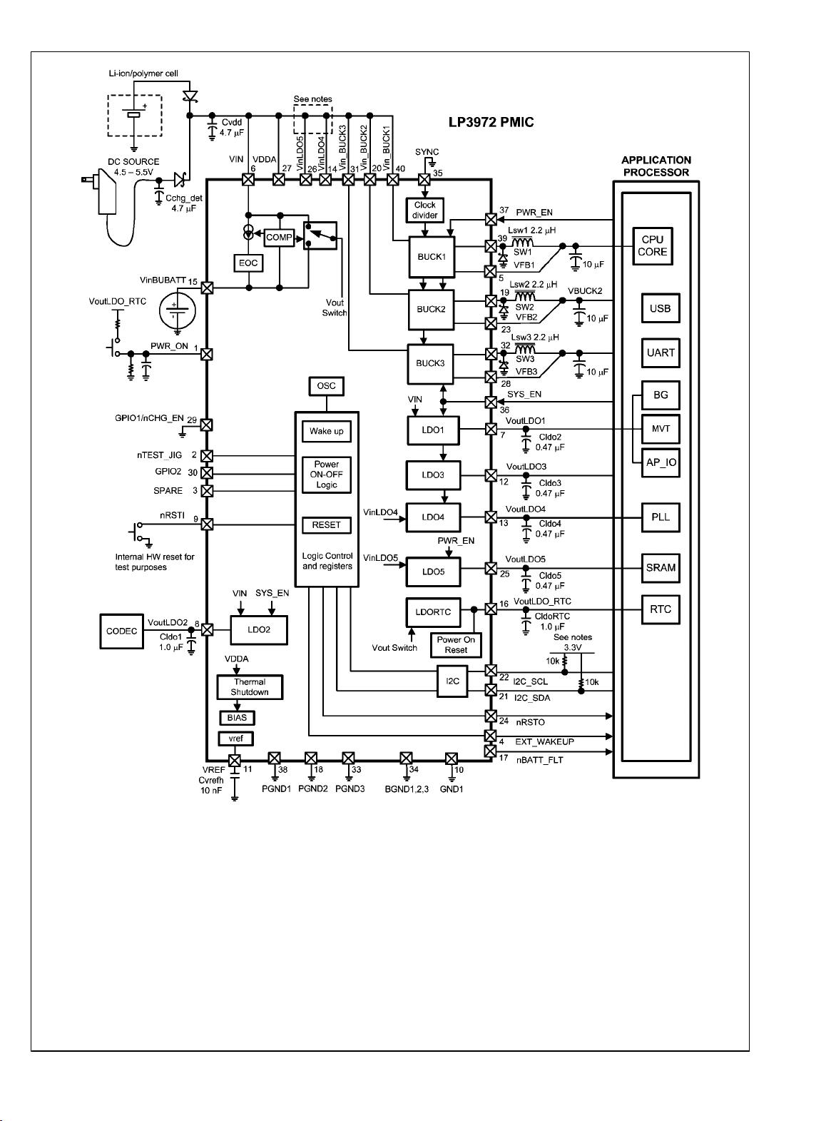
General Description
The LP3972 Flex PMU is a complete power management IC
designed for advanced processors. It contains 5 low noise low
dropout regulators, 3 DC/DC buck converters, a backup bat-
tery charger, real time clock supply regulator [RTC], 2 GPO’s
and high speed I
2
C serial interface to program individual reg-
ulator output voltages as well as offer on/off control. This USB
evaluation board features independent USB powering, virtual
voltmeter bank all in a compact demonstration platform.
Key Features
•
2.7V to 5.5V input voltage range
•
Programmable V
OUT
0.8–3.3 volts
•
Up to 95% efficiency
•
±3% output voltage accuracy
•
1.5A output current [bucks]
Applications
•
Personal Media Players
•
Smart Phones
•
PDA Phones
•
Digital Cameras
LP3972 Evaluation Board Version B
30018301
© 2007 National Semiconductor Corporation 300183 www.national.com
LP3972 USB Evaluation Board version B AN-1621

Evaluation Board/Kit Overview
The LP3972 Evaluation Board supports complete functional
evaluation of the power management IC. The functions of the
chip are controlled by the I
2
C interface. The I
2
C interface on
the rev B and later USB boards are driven via a COP8 micro-
processor which supports a connection via the USB port and
offers chip powering and virtual software voltage measure-
ment of all regulators. In addition, the LP3972 can be powered
directly through the USB port for full function. If high current
Buck testing is desired, an external LI ION cell or PS capable
of supplying 2 amps or more will need to be connected to the
appropriate connector.
The evaluation board/kit consists of:
•
LP3972 Flex_PMU device soldered down in LQA-40 pin
5X5 LD package
•
Full USB interface
•
LED LDO monitoring with current limit resistors
[selectable]
•
External power LDO, Buck output and main battery/supply
connectors offered in heavy duty turret pins and solder
pads
•
Socket for back-up battery
•
Users guide
•
Codeloader Software version .202 or greater [may be sent
via email]
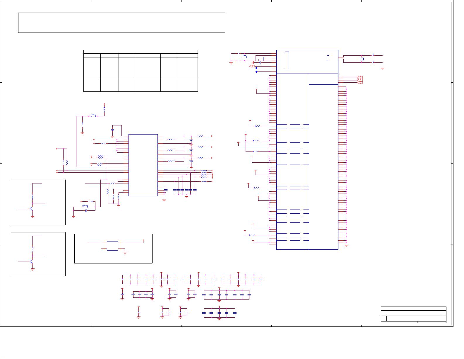
LP3972 Flex_PMU USB Evaluation Board Block Operational Diagram
30018302
www.national.com 2
AN-1621
Pin Description 5X5 package
Pin # Name I/O Type Description
1 PKEY I D CPU Wakeup Input
2 nTJ I D CPU Wakeup Input
3 SP I D CPU Wakeup Input
4 EXT_WAKEUP O D CPU Wakeup Input
5 FB1, Feedback Buck1 I A Buck 1 Feedback
6 V
IN
1 = V
BATT
I P Battery Input for Powering Internal Circuits and LDO1-3
7 LDO_V
OUT
_1 O P LDO1 Output
8 LDO_V
OUT
_2 O P LDO2 Output
9 nRST In I D Chip Reset Input
10 LDO GND 1 G G Ground
11 LDO V
REF
Bypass O A Bypass Capacitor for Reference
12 LDO_V
OUT
_3 O P LDO3 Output
13 LDO_V
OUT
_4 O P LDO4 Output
14 V
IN
LDO_4 I P Input Power for LDO4
15 Back-Up Battery V
IN
I P Back Up Battery Input
16 LDO_V
OUT
_0 (RTC) O P LDO_RTC Output
17 nBatt_FLT O D Main Battery Fault Output
18 PGND Buck2 G G Ground
19 V
OUT
Buck2 O P Buck Switcher2 Output
20 V
IN
Buck2 I P Buck Switcher 2 Battery Input
21 SDA I/O D I
2
C Data Line
22 SCL I D I
2
C Clock Input
23 FB2, Feedback Buck2 I A Buck Switcher 2 Feedback
24 nRST Out O D Reset Output
25 LDO_V
OUT
_5 O P LDO5 Output
26 V
IN
2 (LDO 5 Only) I P Battery Input Power for LDO5
27 VDDA I P Analog Power Input
28 FB3, Feedback Buck3 I A Buck Switcher 3 Feedback
29 GPIO1/nCHG_EN I/O D General Purpose I/O #1/BUBATT Charger EN
30 GPIO2 I/O D General Purpose I/O #2
31 V
IN
Buck3 I P Buck Switcher 3 Battery Input
32 V
OUT
Buck3 I P Buck Switcher 2 Output
33 PGND Buck3 G G Buck3 NMOS Power Ground
34 Buck 1 2 & 3 AVSS/NCHBLK G G Buck1, 2, 3 Analog Ground
35 SYNC (Buck Clock input) I D Buck Switcher External Clock Input
36 Sys_En I D Power Domain Enable
37 Pwr_En I D Power Domain Enable
38 PGND Buck1 G G Buck1 NMOS Power Ground
39 V
OUT
Buck1 O P Buck Switcher 1 Output
40 V
IN
Buck1 I P Buck Switcher 1 Battery Input
A: Analog Pin D: Digital Pin G: Ground Pin P: Power Pin
I: Input Pin I/O: Input/Output Pin O: Output Pin
3 www.national.com
AN-1621

Operating Instructions
The following instructions give general instructions for use of
LP3972 with the evaluation board. Practice standard ESD
protection (ground cable) to prevent any unwanted damaging
ESD events.
1.
Check that the jumpers are in default settings (jumpers
are introduced later in this document).
2.
Load version .202 or later of the codeloader program into
PC.
3.
Connect the USB cable [standard USB AB cable] from
the USB connector to PC port.
4.
Open the codeloader program up, verify that “USB” port
has been selected.
5.
Verify that successful communications link has been
established by toggling “READ ALL”.
6.
If there is no communication, key the USB RST [SW1]
switch once on the board for reboot.
7.
If the voltmeter monitoring function is desired, select
“POLL STATUS”.
8.
LDO/buck outputs may be monitored directly off the
appropriate header output pins.
9.
Note that for full load testing, an external PS must be
connected to TP1/TP2 and jumper J1 must be removed.
This is because the USB port source spec is limited to
500 mA and removing the jumper will disconnect the USB
supply.
10.
PWR EN/SYS En is selectable via codeloader software
assignment.
11.
Hardware reset can be accomplished by pressing the
nREST_In momentary switch.
12.
Battery backup is possible by inserting appropriate
rechargeable cell into supplied holder.
13.
Switches PKEY, nTJ, and SP, are provided for use in
normal evaluation mode.
List of Components
Feb. 8, 2007
Item Qty. Reference Value Pkg. Manuf. Part Number
1 5 C1,C21,CC,CD,CF1 10 µF 0805 Panasonic ECJ2FF1A106Z
2 2 C2,C3 100 µF 3528-21 Kemet T520B107M006ASE040
3 8 C4,C7,C13,C15,C16,C31,CA,
CB
1 µF 0805 Kemet C0805C105K4RACTU
4 6 C5,C6,C8,C9,C25,C29 10 µf 1206 Taiyo-Yuden JMK316BJ106M
5 6 C14,C19,C20,C23,C24,C26 0.47 µF 0805 TDK C2012X7R1E474K
6 2 C17,C18 47 pF 0805 Murata GRM2195C2A470JZ01D
7 4 C22,C30,C32,C33 0.1 µF 0805 Murata GRM21BR71E104KA01L
8 2 C27,C28 15 pF 0805 Yageo 0805CG150J9B200
9 1 BT2 Battery Holder SMT Seiko BH0414
10 1 NOT INSTALLED Backup Battery Micro4 Seiko MS412F
11 4 D6,D7,D10,D11 Schottky PM 457 On Semi MBRM120LT3
12 2 D8 (PWR EN), D9 (SYS EN) Green LED 1206 Lumex SML-LX1206GC-TR
13 9 LDO1(D13), LDO2(D14),
LDO3(D18), LDO4(D17),
LDO5(D19), LDORTC(D16)
D2,D3,D12
Red LED 1206 Lumex SML-LX1206IC-TR
14 2 L1,L2 1 µH Inductor 0805 TDK MLF2012A1R0K
15 3 L3,L4,L5 2.2 µH Inductor SMT Toko FDSE0312
16 1 Q1 XTAL 24 MHz 18 PF SMD Citizen HCM49-24.000MABJT
17 7 R1,R2,R23,R31,R32,
R33,R34
330Ω
0805 SEI 807065R330
18 1 R8
100Ω
0805 NIC NRC10J101TR
19 1 R9
49.9Ω
0805 Rohm MCR10EZHF49R9
20 11 R10,R11,R12,R17,R18,R22,
R24,R26,R27,R36,R37
10K 0805 Yageo 9C08052A1002FKHFT
21 1 R12
0Ω
0805 Yaego 9C08052A0R00JLHFT
22 4 R15,R16,R28,R29
133Ω
0805 Rohm MCR10EZHF1330
23 2 R19,R20
22.1Ω
0805 Vishay-Dale CRCW080522R1ERT1
24 1 R21 1M 0805 Yageo 9C08052A1004JLHFT
25 1 R25 1.5K 0805 Yageo 9C08052A1501FKHFT
www.national.com 4
AN-1621

Item Qty. Reference Value Pkg. Manuf. Part Number
26 1 D1
45.3Ω
0805 Vishay-Dale CRCW080545R3F100
27 5 S1,S2,S3,S4,SW1 Touch Switch SMD Panasonic EVQ-PJU04K
28 1 U1 3.3V Regulator SOT-23 5 NSC LP2981AIM5-3.3
29 1 U2 PMU SQF-40 NSC LP3972
30 1 U3 USB Controller SOIC 28 NSC USBN9604-28M
31 1 U4 Microcontroller TSSOP 48 NSC COP8CBE9IMT9
32 1 U5 2V Regulator SOT-23 5L NSC LP3984IMF-2.0
33 1 U6 Voltage Converter SOT-23-6 NSC LM2664M6
34 1 J1 100 mil Header 2 pos Amp 1 X 2 (4-103239-0-02)
35 1 J2 USB Receptacle 4 pos FCI 61729-0010B
36 1 J3 100 mil Header 4 pos Molex 1 X 4 (22-10-2041)
37 3 J4,J7,J8 100 mil Header 4 pos Amp 2 X 2 (4-103240-0-02)
38 1 J5 100 mil Header 12 pos Amp 2 X 6 (4-103240-0-06)
39 1 J6 GPO/LDO Headers 8 pos Amp 2 X 4 (4-103186-0-04)
40 9 TP9,TP10,TP11,TP16,
TP17,TP18,TP23,TP24,TP25
Test Points 1 pos Amp 1 X 1 (4-103185-0-01)
41 8 TP2,TP4,TP6,TP8,TP13,
TP15,TP20,TP22
Turret Terminal 0.109"L Keystone 1502-2
42 1 LP3972 version B Fab Bare board 4 Layer Rainbow Labs LP3972-B
Powering and Jumpers Selection
The LP3972 USB evaluation platform offers several power
connectors. These connectors are outlined on the table be-
low. In addition, the Evaluation board has jumpers for special
modes and stand-alone use. The default jumper settings are
valid in normal operation and are also outlined below.
Component Use Comment
J5-1 Output for LDO1 Outside Pin of Connector is Grd
J5-2 Output for LDO2 Outside Pin of Connector is Grd
J5-3 Output for LDO3 Outside Pin of Connector is Grd
J5-4 Output for LDO4 Outside Pin of Connector is Grd
J5-6 Output for LDO5 Use LED Pad [Missed Pin]
J5-5 Output for RTC [Real time Clock] Outside Pin of Connector is Grd
J4-1 Input for external wakeup Outside Pin of Connector is Grd
J4-2 Output for nBATT Fault Outside Pin of Connector is Grd
J6-2 Output for nREST Outside Pin of Connector is Grd
J6-3 GPO 1 output Outside Pin of Connector is Grd
J6-4 GPO 2 output Outside Pin of Connector is Grd
J3-1 Cop8 microwire SO Used for Micro Flash Only
J3-2 Cop8 microwire SK Used for Micro Flash Only
J3-3 Cop8 microwire SI Used for Micro Flash Only
J3-4 Cop 8 Grd Used for Micro Flash Only
TP14-15 Output for switcher buck 1 GRD is TP12-13
TP19-20 Output for switcher buck 2 GRD is TP21-22
TP5-6 Output for switcher buck 3 GRD is 7-8
USB USB connector Connect to PC via Supplied Cable
J1 Power usage selection Place Jumper for USB, NO JUMPER for External
Power Input
TP1-2 Connect external V
CC
supply here 3.5-5 volts for high current
testing
Doubles for LI-ION Cell Input, Select Appropriate
J1 Setting [2-3]
5 www.national.com
AN-1621


评论3
最新资源