没有合适的资源?快使用搜索试试~ 我知道了~
资源详情
资源评论
资源推荐
Features
• Serial Peripheral Interface (SPI) Compatible
• Supports SPI Modes 0 (0,0) and 3 (1,1)
– Datasheet describes Mode 0 Operation
• 50 MHz Clock Rate
• Byte Mode and Page Mode Program (1 to 256 Bytes) Operations
• Sector/Block/Page Architecture
– 256 byte Pages per Sector
– Eight 4 Kbyte Sectors per Block
– Four uniform 32 Kbyte Blocks
• Self-timed Sector, Block and Chip Erase
• Product Identification Mode with JEDEC Standard
• Low-voltage Operation
– 2.7V (V
CC
= 2.7V to 3.6V)
• Hardware and Software Write Protection
– Device protection with Write Protect (
WP) Pin
– Write Enable and Write Disable Instructions
– Software Write Protection:
• Upper 1/32, 1/16, 1/8, 1/4, 1/2 or Entire Array
• Flexible Op Codes for Maximum Compatibility
• Self-timed Program Cycle
– 30 µs/Byte Typical
• Single Cycle Reprogramming (Erase and Program) for Status Register
• High Reliability
– Endurance: 10,000 Write Cycles Typical
• 8-lead JEDEC 150mil SOIC and 8-lead Ultra Thin Small Array Package (SAP)
• Die Sales: Waffer Form, Tape and Reel, and Bumped Waffers
Description
The AT25FS010 provides 1,048,576 bits of serial reprogrammable Flash memory
organized as 131,072 words of 8 bits each. The device is optimized for use in many
industrial and commercial applications where low-power and low-voltage operation
are essential. The AT25FS010 is available in a space-saving 8-lead JEDEC SOIC and
8-lead Ultra Thin SAP packages.
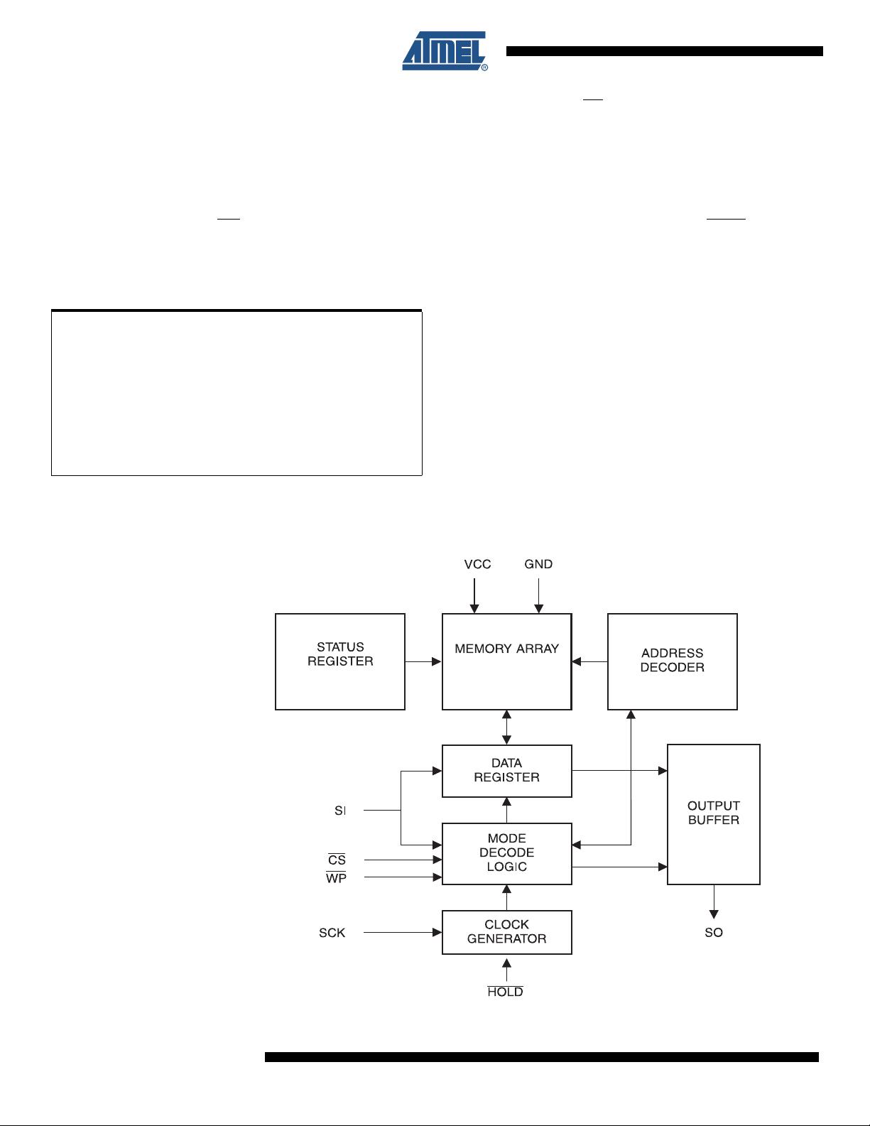
Table 0-1. Pin Configuration
Pin Name Function
CS Chip Select
SCK Serial Data Clock
SI Serial Data Input
SO Serial Data Output
GND Ground
VCC Power Supply
WP Write Protect
HOLD
Suspends Serial
Input
High Speed
Small Sectored
SPI Flash
Memory
1M (131,072 x 8)
AT25FS010
Not Recommended
for New Design
See AT45DB011D
5167E–SFLSH–5/09
8-lead JEDEC SOIC
1
2
3
4
8
7
6
5
CS
SO
WP
GND
VCC
HOLD
SCK
SI
8-lead SAP
1
2
3
4
8
7
6
5
VCC
HOLD
SCK
SI
CS
SO
WP
GND
___
___
_____
Bottom View
2
5167E–SFLSH–5/09
AT25FS010
The AT25FS010 is enabled through the Chip Select pin (CS) and accessed via a 3-wire inter-
face consisting of Serial Data Input (SI), Serial Data Output (SO), and Serial Clock (SCK). All
write cycles are completely self-timed.
BLOCK WRITE protection for upper 1/32, 1/16, 1/8, 1/4, 1/2 or the entire memory array is
enabled by programming the status register. Separate write enable and write disable instruc-
tions are provided for additional data protection. Hardware data protection is provided via the
WP pin to protect against inadvertent write attempts to the status register. The HOLD pin may be
used to suspend any serial communication without resetting the serial sequence.
Figure 1-1. Block Diagram
1. Absolute Maximum Ratings*
Operating Temperature .................................. –40°Cto+85°C
*NOTICE: Stresses beyond those listed under “Absolute
Maximum Ratings” may cause permanent dam-
age to the device. This is a stress rating only and
functional operation of the device at these or any
other conditions beyond those indicated in the
operational sections of this specification is not
implied. Exposure to absolute maximum rating
conditions for extended periods may affect
device reliability.
Storage Temperature.................................... –65°C to +150°C
Voltage on Any Pin
with Respect to Ground ....................................–1.0V to +5.0V
Maximum Operating Voltage ............................................ 4.2V
DC Output Current........................................................ 5.0 mA
131,072x8
3
5167E–SFLSH–5/09
AT25FS010
Note: 1. This parameter is characterized and is not 100% tested.
Note: 1. V
IL
and V
IH
max are reference only and are not tested.
Table 1-1. Pin Capacitance
(1)
Applicable over recommended operating range from T
A
=25°C, f = 1.0 MHz, V
CC
= +3.6V (unless otherwise noted)
Symbol Test Conditions Max Units Conditions
C
OUT
Output Capacitance (SO) 8 pF V
OUT
=0V
C
IN
Input Capacitance (CS, SCK, SI, WP, HOLD) 6 pF V
IN
=0V
Table 1-2. DC Characteristics (Preliminary – Subject to Change)
Applicable over recommended operating range from: T
AI
= –40°Cto+85°C, V
CC
= +2.7V to +3.6V,
T
AC
=0°Cto+70°C, V
CC
= +2.7V to +3.6V (unless otherwise noted)
Symbol Parameter Test Condition Min Typ Max Units
V
CC
Supply Voltage 2.7 3.6 V
I
CC1
Supply Current V
CC
= 3.6V at 20 MHz, SO = Open Read 10.0 17.0 mA
I
CC2
Supply Current V
CC
= 3.6V at 20 MHz, SO = Open Write 15.0 45.0 mA
I
SB
Standby Current V
CC
= 2.7V, CS = V
CC
2.0 10.0 µA
I
IL
Input Leakage V
IN
=0VtoV
CC
-3.0 3.0 µA
I
OL
Output Leakage V
IN
=0VtoV
CC
,T
AC
=0°Cto70°C -3.0 3.0 µA
V
IL
(1)
Input Low Voltage -0.6 V
CC
x 0.3 V
V
IH
(1)
Input High Voltage V
CC
x 0.7 V
CC
+ 0.5 V
V
OL
Output Low Voltage
2.7V ≤ V
CC
≤ 3.6V
I
OL
= 0.15 mA 0.2 V
V
OH
Output High Voltage I
OH
= -100 µA V
CC
- 0.2 V
4
5167E–SFLSH–5/09
AT25FS010
Notes: 1. The programming time for n bytes will be equal tonxt
BPC
.
2. This parameter is ensured by characterization at 3.0v, 25c only.
3. One write cycle consists of erasing a sector, followed by programming the same sector.
Table 1-3. AC Characteristics (Preliminary – Subject to Change)
Applicable over recommended operating range from T
A
= –40°Cto+85°C, V
CC
= +2.7V to +3.6V
C
L
= 1 TTL Gate and 30 pF (unless otherwise noted)
Symbol Parameter Min Typ Max Units
f
SCK
SCK Clock Frequency 0 50 MHz
t
RI
Input Rise Time 5 ns
t
FI
Input Fall Time 5 ns
t
WH
SCK High Time 9 ns
t
WL
SCK Low Time 9 ns
t
CS
CS High Time 100 ns
t
CSS
CS Setup Time 5 ns
t
CSH
CS Hold Time 5 ns
t
SU
Data In Setup Time 5 ns
t
H
Data In Hold Time 5 ns
t
HD
Hold Setup Time 5 ns
t
CD
Hold Hold Time 5 ns
t
V
Output Valid 9ns
t
HO
Output Hold Time 0 ns
t
LZ
Hold to Output Low Z 9 ns
t
HZ
Hold to Output High Z 9 ns
t
DIS
Output Disable Time 9 ns
t
se
Sector Erase Time 50 200 ms
t
be
Block Erase Time 200 500 ms
t
ce
Chip Erase Time 1.6 4 s
t
SR
Status Register Write Cycle Time 60 ms
t
BPC
Byte Program Cycle Time
(1)
30 50 µs
Endurance
(2)
10K Write Cycles
(3)
5
5167E–SFLSH–5/09
AT25FS010
2. Serial Interface Description
MASTER: The device that generates the serial clock.
SLAVE: Because the Serial Clock pin (SCK) is always an input, the AT25FS010 always oper-
ates as a slave.
TRANSMITTER/RECEIVER: The AT25FS010 has separate pins designated for data transmis-
sion (SO) and reception (SI).
MSB: The Most Significant Bit (MSB) is the first bit transmitted and received.
SERIAL OP-CODE: After the device is selected with CS going low, the first byte will be
received. This byte contains the op-code that defines the operations to be performed.
INVALID OP-CODE: If an invalid op-code is received, no data will be shifted into the
AT25FS010, and the serial output pin (SO) will remain in a high impedance state until the falling
edge of
CS is detected again. This will reinitialize the serial communication.
CHIP SELECT: The AT25FS010 is selected when the CS pin is low. When the device is not
selected, data will not be accepted via the SI pin, and the serial output pin (SO) will remain in a
high impedance state.
HOLD: The HOLD pin is used in conjunction with the CS pin to select the AT25FS010. When
the device is selected and a serial sequence is underway, HOLD can be used to pause the serial
communication with the master device without resetting the serial sequence. To pause, the
HOLD pin must be brought low while the SCK pin is low. To resume serial communication, the
HOLD pin is brought high while the SCK pin is low (SCK may still toggle during HOLD). Inputs to
the SI pin will be ignored while the SO pin is in the high impedance state.
WRITE PROTECT: The AT25FS010 has a write lockout feature that can be activated by assert-
ing the write protect pin (WP). When the lockout feature is activated, locked-out sectors will be
READ only. The write protect pin will allow normal read/write operations when held high. When
the WP is brought low and WPEN bit is “1”, all write operations to the status register are inhib-
ited. WP going low while CS is still low will interrupt a write to the status register. If the internal
status register write cycle has already been initiated, WP going low will have no effect on any
write operation to the status register. The WP pin function is blocked when the WPEN bit in the
status register is “0”. This will allow the user to install the AT25FS010 in a system with the WP
pin tied to ground and still be able to write to the status register. All WP pin functions are enabled
when the WPEN bit is set to “1”.
剩余23页未读,继续阅读
knightdream
- 粉丝: 1
- 资源: 6
上传资源 快速赚钱
- 我的内容管理 展开
- 我的资源 快来上传第一个资源
- 我的收益 登录查看自己的收益
- 我的积分 登录查看自己的积分
- 我的C币 登录后查看C币余额
- 我的收藏
- 我的下载
- 下载帮助
安全验证
文档复制为VIP权益,开通VIP直接复制
信息提交成功
评论2