LT1117-5.pdf
需积分: 0 117 浏览量
2008-07-08
11:28:57
上传
评论 1
收藏 196KB PDF 举报

1
LT1117/LT1117-2.85
LT1117-3.3/LT1117-5
800mA Low Dropout
Positive Regulators
Adjustable and Fixed 2.85V,
3.3V, 5V
Active Terminator for SCSI-2 Bus
Dropout Voltage (V
IN
– V
OUT
)
■
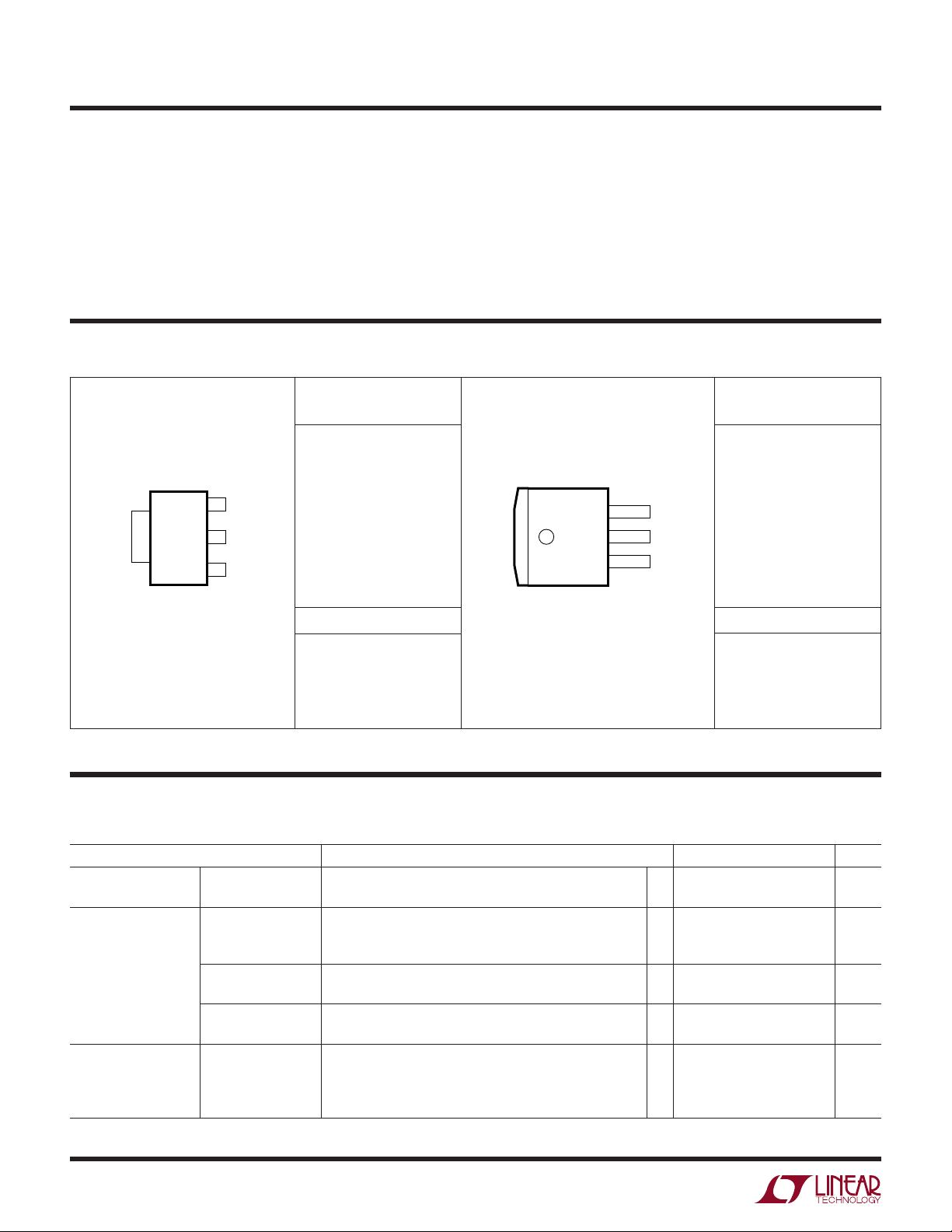
Space Saving SOT-223 Surface Mount Package
■
3-Terminal Adjustable or Fixed 2.85V, 3.3V, 5V
■
Output Current of 800mA
■
Operates Down to 1V Dropout
■
Guaranteed Dropout Voltage at Multiple Current Levels
■
0.2% Line Regulation Max
■
0.4% Load Regulation Max
The LT
®
1117 is a positive low dropout regulator designed
to provide up to 800mA of output current. The device is
available in an adjustable version and fixed output voltages
of 2.85V, 3.3V and 5V. The 2.85V version is designed
specifically to be used in Active Terminators for the SCSI
bus. All internal circuitry is designed to operate down to 1V
input to output differential. Dropout voltage is guaranteed
at a maximum of 1.2V at 800mA, decreasing at lower load
currents. On chip trimming adjusts the reference/output
voltage to within ±1%. Current limit is also trimmed in
order to minimize the stress on both the regulator and the
power source circuitry under overload conditions.
The low profile surface mount SOT-223 package allows
the device to be used in applications where space is
limited. The LT1117 requires a minimum of 10µF of output
capacitance for stability. Output capacitors of this size or
larger are normally included in most regulator designs.
Unlike PNP type regulators where up to 10% of the output
current is wasted as quiescent current, the quiescent
current of the LT1117 flows into the load, increasing
efficiency.
■
Active SCSI Terminators
■
High Efficiency Linear Regulators
■
Post Regulators for Switching Supplies
■
Battery Chargers
■
5V to 3.3V Linear Regulators
FEATURES
DESCRIPTIO
U
APPLICATIO S
U
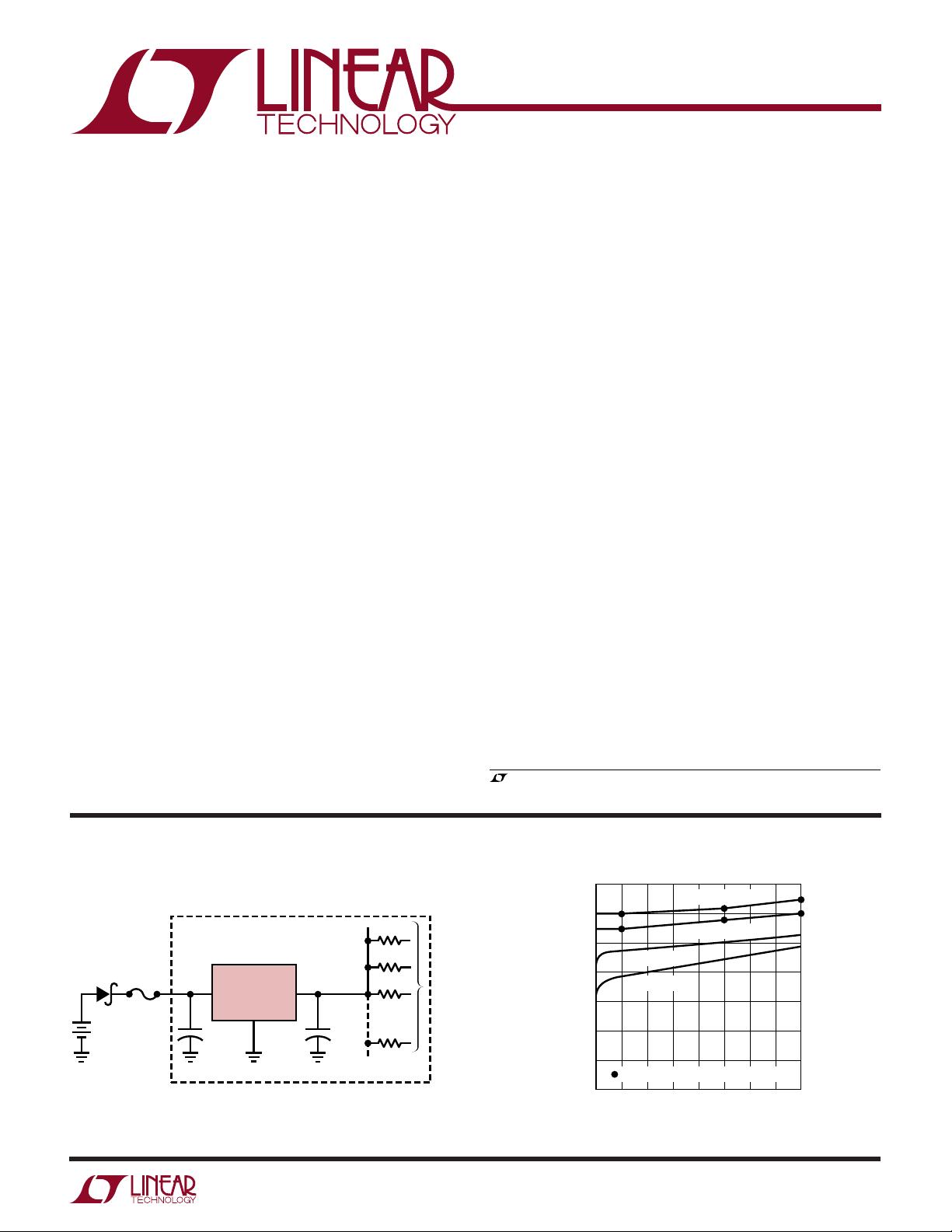
TYPICAL APPLICATIO
U
, LTC and LT are registered trademarks of Linear Technology Corporation.
18 TO 27
LINES
LT1117 • TA01
10µF
110Ω
110Ω
110Ω
110Ω
4.75V TO
5.25V
22µF
LT1117-2.85
IN
GND
OUT
+ +
OUTPUT CURRENT (mA)
0
0
DROPOUT VOLTAGE (V)
0.2
0.4
0.6
0.8
1.0
1.4
100 400 600 800
LT1117 • TPC01
1.2
200 300 500 700
T
J
= 25°C
T
J
= 125°C
INDICATES GUARANTEED TEST POINT
0°C ≤ T
J
≤ 125°C
–40°C ≤ T
J
< 0°C
剩余11页未读,继续阅读


评论0
最新资源