
πPM Tech PMF410816C/PMF510816C
Rev 1.0
2
March 2015
1GBIT DDRIII DRAM
Features
JEDEC DDR3 Compliant
8n Prefetch Architecture
Differential Clock(CK, /CK) and Data trobe(DQS,
/DQS)
Double-data rate on DQs, DQS, DM
Data Integrity
Auto Self Refresh (ASR) by DRAM built-in TS
Auto Refresh and Self Refresh Modes
Power Saving Mode
Partial Array Self Refresh (PASR)
1
Power Down Mode
Signal Integrity
Configurable DS for system compatibility
Configurable On-Die Termination
ZQ Calibration for DS/ODT impedance accuracy
via external ZQ pad (240 ohm ± 1%)
Signal Synchronization
Write Leveling via MR settings
7
Read Leveling via MPR
Interface and Power Supply
SSTL_15 for DDR3:VDD/VDDQ=1.5V(±0.075V)
SSTL_135
4
for DDR3L:VDD/VDDQ=1.35V (-
0.067/+0.1V)
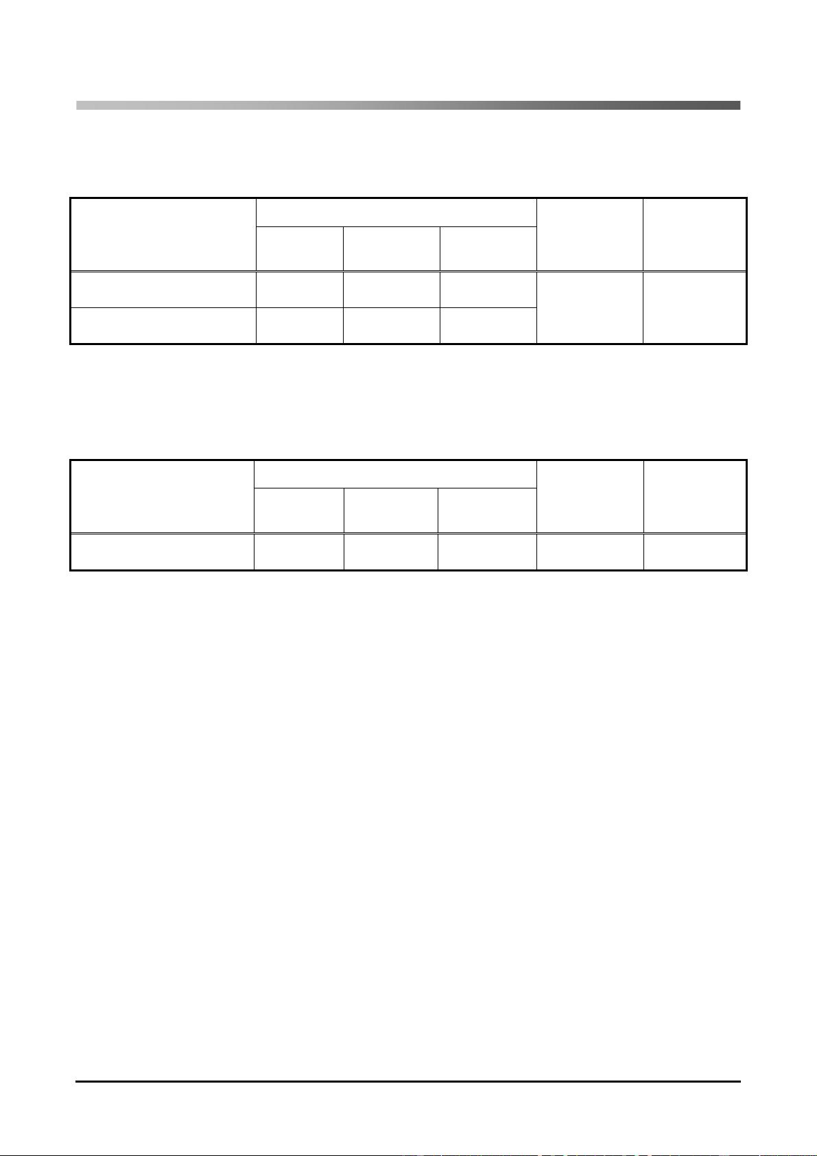
Options
Speed Grade ( DataRate/CL-tRCD-tRP)
2,3
1866 Mbps / 13-13-13
1600 Mbps / 11-11-11
Temperature Range (Tc)
2
Commercial Grade = 0
℃
to + 95
℃
Programmable functions
CAS Latency (5/6/7/8/9/10/11/12/13/14)
CAS Write Latency (5/6/7/8/9/10)
Additive Latency (0/CL-1/CL-2)
Write Recovery Time (5/6/7/8/10/12/14/16)
Burst Type (Sequential/Interleaved)
Burst Length (BL8/BC4/BC4 or 8 on the fly)
Self RefreshTemperature
Range(Normal/Extended)
Output Driver Impedance (34/40)
On-Die Termination of Rtt_Nom(20/30/40/60/120)
On-Die Termination of Rtt_WR(60/120)
Precharge Power Down (slow/fast)
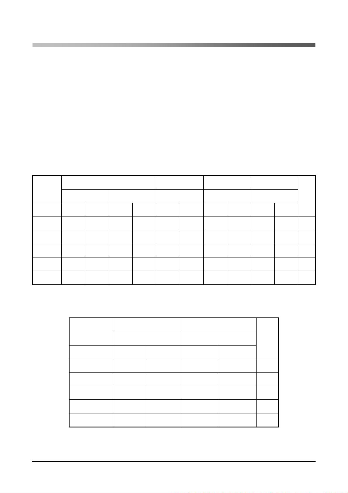
Density information
Lead-free RoHS compliance and Halogen-free
1Gb
(Org / Package)
Length x Width
(mm)
Ball pitch
(mm)
64MX16 96 VFBGA 9.00 x 14.00 0.80
Density and Addressing
Configuration
64 Mb x 16
Bank Address
BA0 – BA2
Auto Precharge
A10/AP
Row Address
A0 - A12
Column Address
A0 - A9
Page Size
2 KB
tREFI(us)
5
Tc<=85℃:7.8, Tc>85℃:3.9
tRFC(ns)
6
110ns


评论0
最新资源