ADSemiconductor
®
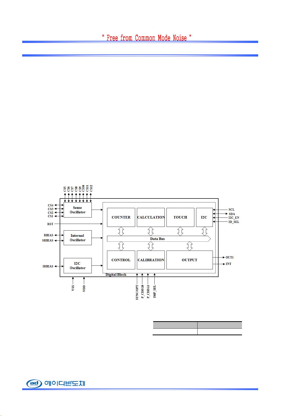
TSM12 (12-CH Auto Sensitivity Calibration Capacitive Touch Sensor)
AD Semiconductor Confidential 4 / 32
Content
General ....................................................................................................................................... 2
Revision History ........................................................................................................................ 3
1 Pin Configuration ............................................................................................................... 5
2 Pin Description ................................................................................................................... 6
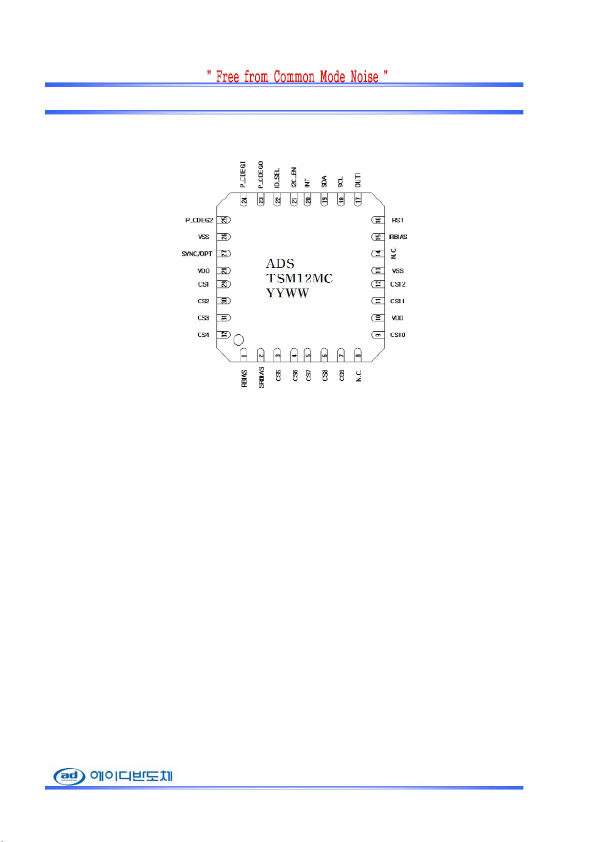
2.1 Pin Map (32 MLF package) .................................................................................. 7
3 Absolute Maximum Rating ................................................................................................ 8
4 ESD & Latch-up Characteristics ........................................................................................ 8
4.1 ESD Characteristics .............................................................................................. 8
4.2 Latch-up Characteristics ....................................................................................... 8
5 Electrical Characteristics .................................................................................................... 9
6 TSM12 Implementation .................................................................................................... 10
6.1 RBIAS & SRBIAS implementation ................................................................... 10
6.2 CS implementation ............................................................................................. 11
6.3 SYNC/OPT implementation ............................................................................... 12
6.4 P_CDEG2 , P_CDEG1, P_CDEG0 implementation .......................................... 13
6.5 RESET implementation ...................................................................................... 14
7 I
2
C Interface ...................................................................................................................... 15
7.1 IRBIAS Implementation ..................................................................................... 15
7.2 Start & stop condition ......................................................................................... 16
7.3 Data validity........................................................................................................ 17
7.4 Byte format ......................................................................................................... 17
7.5 Acknowledge ...................................................................................................... 17
7.6 First byte ............................................................................................................. 18
7.7 Transferring data ................................................................................................. 19
7.8 I
2
C write and read operations in normal mode ................................................... 20
8 TSM12 control register list ............................................................................................... 21
8.1 I
2
C Register Map ................................................................................................ 21
8.2 Details ................................................................................................................. 22
9 Recommended TSM12 Initialize Flow (Example) ........................................................... 26
10 Recommended Circuit Diagram ....................................................................................... 27
10.1 Application Example in clean power environment ............................................ 27
10.2 Application Example in noisy environment ....................................................... 28
10.3 Example – Power Line Split Strategy PCB Layout .......................................................... 29
11 MECHANICAL DRAWING ........................................................................................... 30
11.1 Mechanical Drawing of TSM12M (32 MLF) ..................................................... 30
12 MARKING DESCRIPTION ............................................................................................ 31
12.1 Marking Description of TSM12M (32 MLF) ..................................................... 31
NOTES: ................................................................................................................................... 32