没有合适的资源?快使用搜索试试~ 我知道了~
SCT2613TVBR 产品规格书pdf
1 下载量 94 浏览量
2024-03-20
11:37:51
上传
评论
收藏 1.83MB PDF 举报
温馨提示
试读
21页
SCT2613TVBR 4.5V-60V Vin,1A,高效降压DCDC转换器
资源推荐
资源详情
资源评论
SCT2613
Rev.1.1
For more information www.silicontent.com © 2021 Silicon Content Technology Co., Ltd. All Rights Reserved 1
Product Folder Links: SCT2613
芯洲科技
Silicon Content Technology
4.5V-60V Vin, 1A, High Efficiency Step-down DCDC Converter
FEATURES
Wide Input Range: 4.5V-60V
Continuous Output Current: 1A
0.765V ±2.5% Feedback Reference Voltage
Integrated 500mΩ High-Side
Low Quiescent Current: 80uA
Pulse Skipping Mode (PSM) in light load
80ns Minimum On-time
6ms Internal Soft-start Time
Internal compensation
Switching Frequency 480KHz
Precision Enable Threshold for Programmable
Input Voltage Under-Voltage Lock Out Protection
(UVLO) Threshold and Hysteresis
Low Dropout Mode Operation
Over-voltage and Over-Temperature Protection
Available in an TSOT23-6L Package
APPLICATIONS
12-V, 24-V, 48-V Industry and Telecom Power
System
Industrial Automation and Motor Control
Vehicle Accessories
Portable Handheld Instruments
Portable Media Players
DESCRIPTION
The SCT2613 is 1A buck converter with wide input
voltage, ranging from 4.5V to 60V, which integrates an
500mΩ high-side MOSFET. The SCT2613, adopting
the peak current mode control, supports the Pulse
Skipping Modulation (PSM) with 80uA low quiescent
current which assists the converter on achieving high
efficiency at light load or standby condition.
The SCT2613 features fixed 480KHz switching
frequency, which minimizes the external off chip
passive components size and reduces the output
ripple. The SCT2613 allows power conversion from
high input voltage to low output voltage with a minimum
80ns on-time of high-side MOSFET and also supports
low dropout operation with a low voltage difference
from input to output.
The device offers fixed 6ms soft start to prevent inrush
current during the startup of output voltage ramping,
and compensation circuits are implemented internally
which allows the device to be used with minimized
external components.
The SCT2613 provides cycle-by-cycle current limit,
thermal shutdown protection, output over-voltage
protection and input voltage under-voltage protection.
The device is available in an TSOT23-6L package.
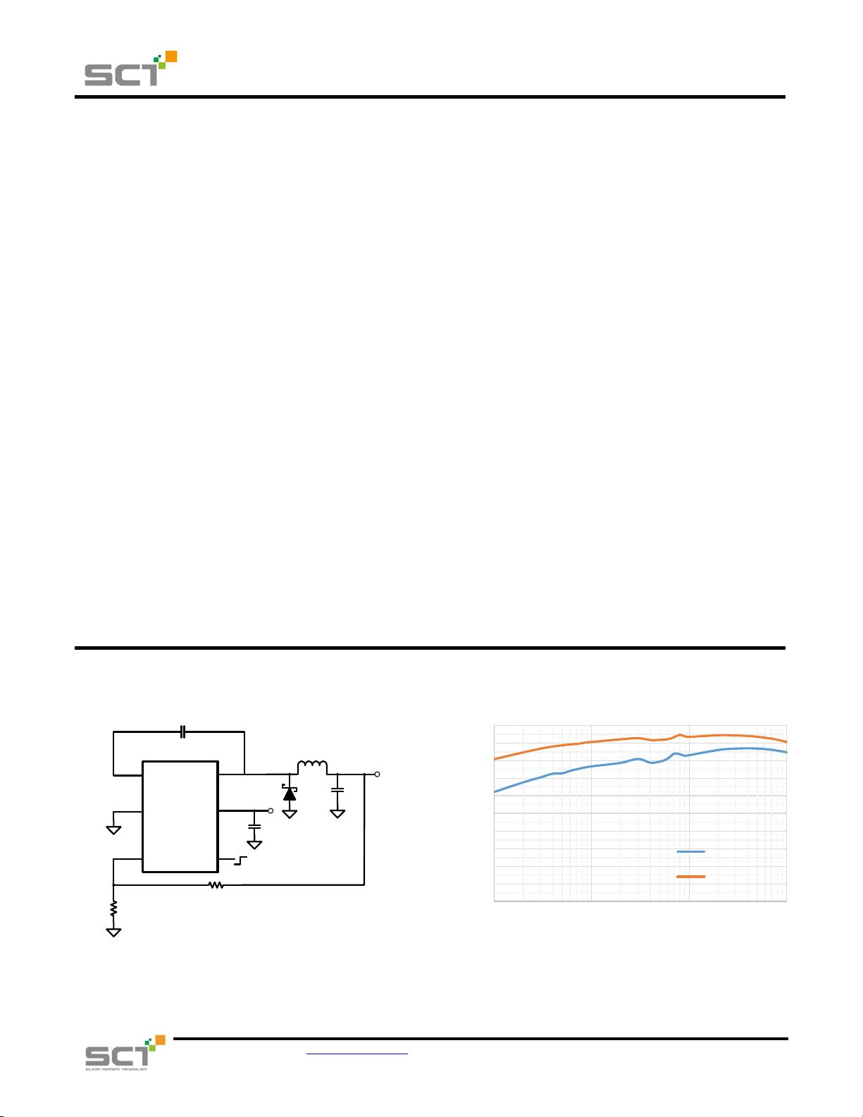
TYPICAL APPLICATION
SW
BST
GND
VIN
EN
V
IN
L1
C1
C3
R1
R2
V
OUT
FB
C2
D1
ON
OFF
4.5V-60V, Asyncronous Buck Converter
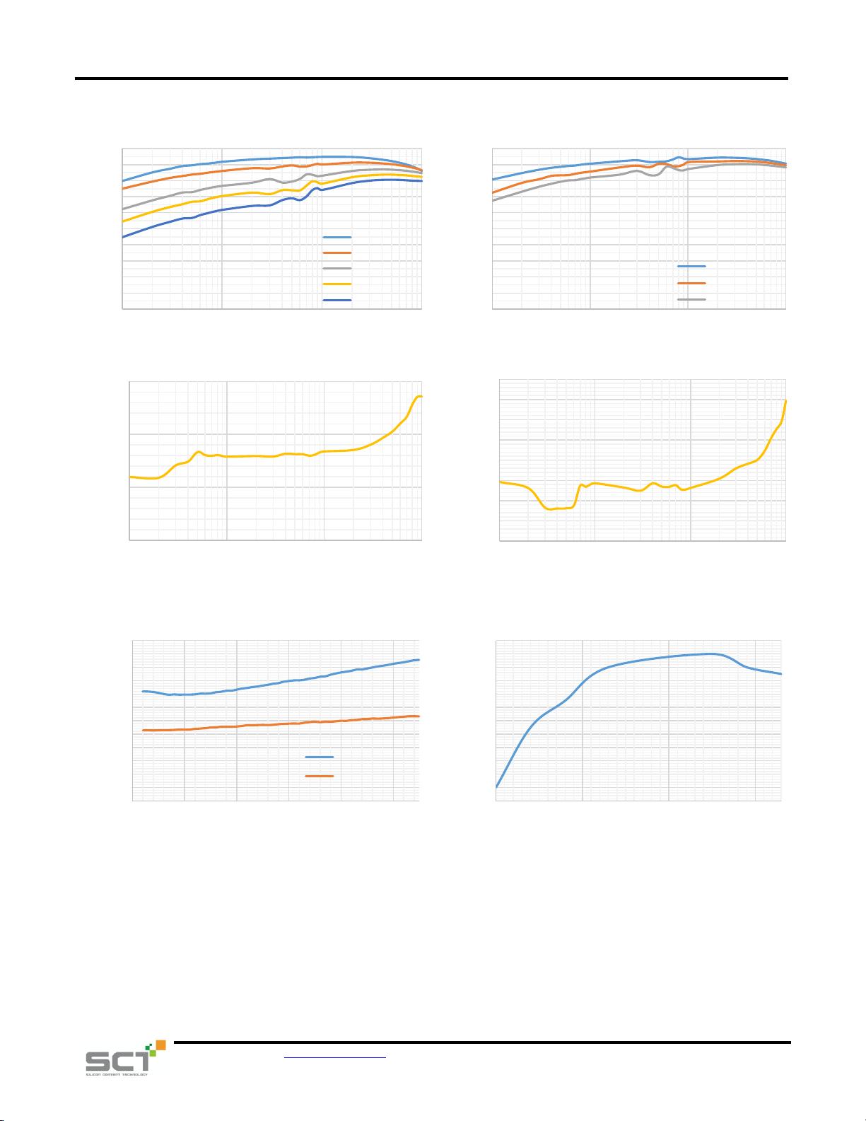
Efficiency, Vin=24V
0
10
20
30
40
50
60
70
80
90
100
0.001 0.01 0.1 1
Efficiency(%)
Output current(A)
24VIN 5VOUT
24VIN 12VOUT
SCT2613
2 For more information www.silicontent.com © 2021 Silicon Content Technology Co., Ltd. All Rights Reserved
Product Folder Links: SCT2613
REVISION HISTORY
NOTE: Page numbers for previous revisions may differ from page numbers in the current version.
Revision 1.0: Production
Revision 1.1: Update Figure 8, remove Zener diode
DEVICE ORDER INFORMATION
PART NUMBER
PACKAGE MARKING
PACKAGE DISCRIPTION
SCT2613TVB
2613
TSOT23-6L
1) For Tape & Reel, Add Suffix R (e.g. SCT2613TVBR)
ABSOLUTE MAXIMUM RATINGS
Over operating free-air temperature unless otherwise noted
(1)
PIN CONFIGURATION
DESCRIPTION
MIN
MAX
UNIT
1
2
3 4
5
6
BST
GND
FB
EN
VIN
SW
Figure 1. 6-Lead Plastic TSOT23-6L
VIN, EN
-0.3
65
V
BST
-0.3
72
V
SW
-1
65
V
BST-SW
-0.3
6
V
FB
-0.3
6
V
Operating junction temperature TJ
(2)
-40
150
°C
Storage temperature TSTG
-65
150
°C
(1) Stresses beyond those listed under Absolute Maximum Rating may cause device permanent damage. The device is not guaranteed to
function outside of its Recommended Operation Conditions.
(2) The IC includes over temperature protection to protect the device during overload conditions. Junction temperature will exceed 150°C
when over temperature protection is active. Continuous operation above the specified maximum operating junction temperature will
reduce lifetime.
PIN FUNCTIONS
NAME
NO.
PIN FUNCTION
BST
1
Power supply bias for high-side power MOSFET gate driver. Connect a 0.1uF capacitor
from BOOT pin to SW pin. Bootstrap capacitor is charged when SW voltage is low.
GND
2
Ground
FB
3
Buck converter output feedback sensing voltage. Connect a resistor divider from VOUT
to FB to set up output voltage. The device regulates FB to the internal reference of
0.765V typically.
EN
4
Enable pin to the regulator with internal pull-up current source. Pull below 1.13V to
disable the converter. Float or connect to VIN to enable the converter. The tap of resistor
divider from VIN to GND connecting EN pin can adjust the input voltage lockout
threshold.
VIN
5
Input supply voltage. Connect a local bypass capacitor from VIN pin to GND pin
SW
6
Regulator switching output. Connect SW to an external power inductor
SCT2613
For more information www.silicontent.com © 2021 Silicon Content Technology Co., Ltd. All Rights Reserved 3
Product Folder Links: SCT2613
RECOMMENDED OPERATING CONDITIONS
Over operating free-air temperature range unless otherwise noted
PARAMETER
DEFINITION
MIN
MAX
UNIT
V
IN
Input voltage range
4.5
60
V
V
OUT
Output voltage range
0.765
57
V
T
J
Operating junction temperature
-40
150
°C
ESD RATINGS
PARAMETER
DEFINITION
MIN
MAX
UNIT
V
ESD
Human Body Model(HBM), per ANSI-JEDEC-JS-001-2014
specification, all pins
(1)
-2
+2
kV
Charged Device Model(CDM), per ANSI-JEDEC-JS-002-
2014 specification, all pins
(2)
-0.5
+0.5
kV
(1) JEDEC document JEP155 states that 500V HBM allows safe manufacturing with a standard ESD control process.
(2) JEDEC document JEP157 states that 250V CDM allows safe manufacturing with a standard ESD control process.
THERMAL INFORMATION
PARAMETER
THERMAL METRIC
TSOT23-6L
UNIT
R
θJA
Junction to ambient thermal resistance
(1)
102
°C/W
R
θJC
Junction to case thermal resistance
(1)
36.9
(1) SCT provides R
θJA
and R
θJC
numbers only as reference to estimate junction temperatures of the devices. R
θJA
and R
θJC
are not a
characteristic of package itself, but of many other system level characteristics such as the design and layout of the printed circuit
board (PCB) on which the SCT2613 is mounted, thermal pad size, and external environmental factors. The PCB board is a heat sink
that is soldered to the leads and thermal pad of the SCT2613. Changing the design or configuration of the PCB board changes the
efficiency of the heat sink and therefore the actual R
θJA
and R
θJC
.
SCT2613
4 For more information www.silicontent.com © 2021 Silicon Content Technology Co., Ltd. All Rights Reserved
Product Folder Links: SCT2613
ELECTRICAL CHARACTERISTICS
V
IN
=24V, T
J
=-40°C~125°C, typical value is tested under 25°C.
SYMBOL
PARAMETER
TEST CONDITION
MIN
TYP
MAX
UNIT
Power Supply
V
IN
Operating input voltage
4.5
60
V
V
IN_UVLO
Input UVLO Threshold
V
IN
rising
4.23
4.45
V
Hysteresis
200
mV
I
SHDN
Shutdown current from VIN pin
EN=0, no load
1.65
5
μA
I
Q
Quiescent current from VIN pin
EN floating, no load,
non-switching
80
μA
Power MOSFETs
R
DSON_H
High-side MOSFET on-resistance
V
BOOT
-V
SW
=5V
500
mΩ
Reference
V
REF
Reference voltage of FB
0.746
0.765
0.784
V
Current Limit and Over Current Protection
I
LIM_HS
High-side power MOSFET peak
current limit threshold
1.5
2
2.4
A
Enable and Soft Startup
V
EN_H
Enable high threshold
1.223
1.4
V
V
EN_L
Enable low threshold
0.9
1.13
V
V
EN_HYS
Enable threshold hysteresis
93
mV
I
EN_L
Enable pin pull-up current
EN=1V
1
μA
I
EN_H
Enable pin pull-up current
EN=1.5V
4
uA
T
SS
Soft start time
6
ms
Switching Frequency
F
SW
Switching frequency
394
480
566
kHz
t
ON_MIN
Minimum on-time
V
IN
=12V
80
ns
Protection
V
OVP
Feedback overvoltage with respect to
V
FB
/V
REF
rising
110
%
reference voltage
V
FB
/V
REF
falling
105
%
V
BOOTUV
BOOT-SW UVLO threshold
BOOT-SW falling
2.2
V
Hysteresis
250
mV
T
SD
Thermal shutdown threshold*
T
J
rising
173
°C
Hysteresis
10
°C
*Derived from bench characterization
SCT2613
For more information www.silicontent.com © 2021 Silicon Content Technology Co., Ltd. All Rights Reserved 5
Product Folder Links: SCT2613
TYPICAL CHARACTERISTICS
Figure 2. Efficiency vs Load Current, Vout=5V
Figure 3. Efficiency vs Load Current, Vout=12V
Figure 4. Load Regulation, Vin=24V, Vout=5V
Figure 5. Load Regulation, Vin=24V, Vout=12V
Figure 6. Line Regulation
Figure 7. HS Current Limit VS Temperature
0
10
20
30
40
50
60
70
80
90
100
0.001 0.01 0.1 1
Efficiency(%)
Output curren (A)
7VIN 5VOUT
12VIN 5VOUT
24VIN 5VOUT
36VIN 5VOUT
48VIN 5VOUT
0
10
20
30
40
50
60
70
80
90
100
0.001 0.01 0.1 1
Efficiency(%)
Output curren (A)
24VIN 12VOUT
36VIN 12VOUT
48VIN 12VOUT
4.97
4.98
4.99
5
0.001 0.01 0.1 1
Output Voltage(V)
Output curren (A)
11.98
11.99
12
12.01
12.02
12.03
12.04
12.05
12.06
0.001 0.01 0.1 1
Output Voltage(V)
Output curren (A)
4.96
4.965
4.97
4.975
4.98
4.985
4.99
4.995
5
5.005
5.01
5.015
5.02
5 15 25 35 45 55
Output Voltage(V)
Input Voltage(V)
5VOUT IOUT=1A
5VOUT IOUT=0.1A
1.8
1.82
1.84
1.86
1.88
1.9
1.92
1.94
1.96
1.98
2
2.02
2.04
-40 10 60 110
Current Limit(A)
Temperature(℃)
剩余20页未读,继续阅读
资源评论
宏源世纪-niki
- 粉丝: 445
- 资源: 87
上传资源 快速赚钱
- 我的内容管理 展开
- 我的资源 快来上传第一个资源
- 我的收益 登录查看自己的收益
- 我的积分 登录查看自己的积分
- 我的C币 登录后查看C币余额
- 我的收藏
- 我的下载
- 下载帮助
最新资源
- 技术面试最后反问面试官的话 校招面试非技术问题有哪些 非技术问题如何回答.png
- NB-IOT-BC26全网通模块Altium+ CADENCE +PADS三种格式(原理图SCH+PCB封装库)文件.zip
- 基于微信小程序开发的校园失物招领系统源码毕业设计(优质项目源码).zip
- 词向量是一种将自然语言中的单词转换为数值向量的技术,它能够捕捉词义和上下文信息
- nmap与masscan的简单使用
- MyBatis动态SQL.pdf
- 基于stm32单片机protues仿真的温湿度控制系统设计(仿真图、源代码)
- 词向量:自然语言处理的基石
- mybatis动态sql
- 40G微信小程序开发教程(工具插件+视频教程)
资源上传下载、课程学习等过程中有任何疑问或建议,欢迎提出宝贵意见哦~我们会及时处理!
点击此处反馈
安全验证
文档复制为VIP权益,开通VIP直接复制
信息提交成功