SCT2A10ASTER 产品规格书pdf
77 浏览量
2024-03-20
11:34:26
上传
评论
收藏 1.2MB PDF 举报

SCT2A10A
For more information www.silicontent.com © 2019 Silicon Content Technology Co., Ltd. All Rights Reserved 1
Product Folder Links: SCT2A10A
SILICON CONTENT
TECHNOLOGY
4.5V-100V Vin, 0.6A, High Efficiency Synchronous Step-down DCDC
Converter with Programmable Frequency
FEATURES
Wide Input Range: 4.5V-100V
0.6A Continuous Output Current
0.8V ±1% Feedback Reference Voltage
Integrated 750mΩ High-Side and 500mΩ Low-
Side Power MOSFETs
Pulse Frequency Modulation (PFM) with 100uA
Quiescent Current in Sleep Mode
4ms Internal Soft-start Time
Adjustable Frequency 300KHz to 800KHz
Precision Enable Threshold for Programmable
Input Voltage Under-Voltage Lock Out Protection
(UVLO) Threshold and Hysteresis
Cycle-by-Cycle Current Limiting
Over-Voltage Protection
Over-Temperature Protection
Available in an ESOP-8 Package
APPLICATIONS
E-Tools
E-bike, Scooter
GPS Tracker
DESCRIPTION
The SCT2A10A is 0.6A synchronous buck converters
with wide input voltage, ranging from 4.5V to 100V,
which integrates an 750mΩ high-side MOSFET and a
500mΩ low-side MOSFET. The SCT2A10A, adopting
the constant-on time (COT) mode control, supports the
PFM with typical 100uA low quiescent current which
assists the converter on achieving high efficiency at
light load or standby condition.
The SCT2A10A features programmable switching
frequency from 300 kHz to 800kHz, which provides the
flexibility to optimize either efficiency or external
component size.
The SCT2A10A offers cycle-by-cycle current limit and
hiccup over current protection, thermal shutdown
protection, output over-voltage protection and input
voltage under-voltage protection. The device is
available in an 8-pin thermally enhanced SOP-8
package.
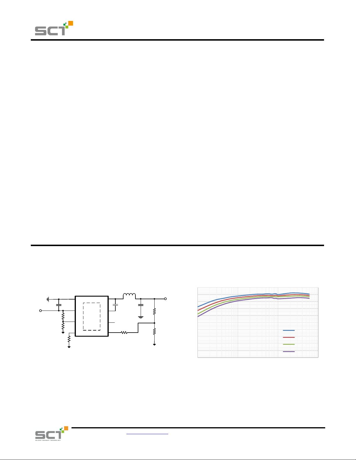
TYPICAL APPLICATION
L1
R3
R4
R5
C2
V
OU T
R1
R2
C1
C4
EN
RT
SW
NC
FB
V
IN
SCT2A10A
BST
GND
VIN
R6
Typical Application Efficiency, V
OUT
=12V
0
10
20
30
40
50
60
70
80
90
100
0.001 0.01 0.1 1
Efficiency(%)
Output Current(A)
Vin=36V
Vin=48V
Vin=60V
Vin=72V
剩余17页未读,继续阅读
资源评论


