
L293, L293D
QUADRUPLE HALF-H DRIVERS
SLRS008C − SEPTEMBER 1986 − REVISED NOVEMBER 2004
1
POST OFFICE BOX 655303 • DALLAS, TEXAS 75265
D Featuring Unitrode L293 and L293D
Products Now From Texas Instruments
D Wide Supply-Voltage Range: 4.5 V to 36 V
D Separate Input-Logic Supply
D Internal ESD Protection
D Thermal Shutdown
D High-Noise-Immunity Inputs
D Functionally Similar to SGS L293 and
SGS L293D
D Output Current 1 A Per Channel
(600 mA for L293D)
D Peak Output Current 2 A Per Channel
(1.2 A for L293D)
D Output Clamp Diodes for Inductive
Transient Suppression (L293D)
description/ordering information
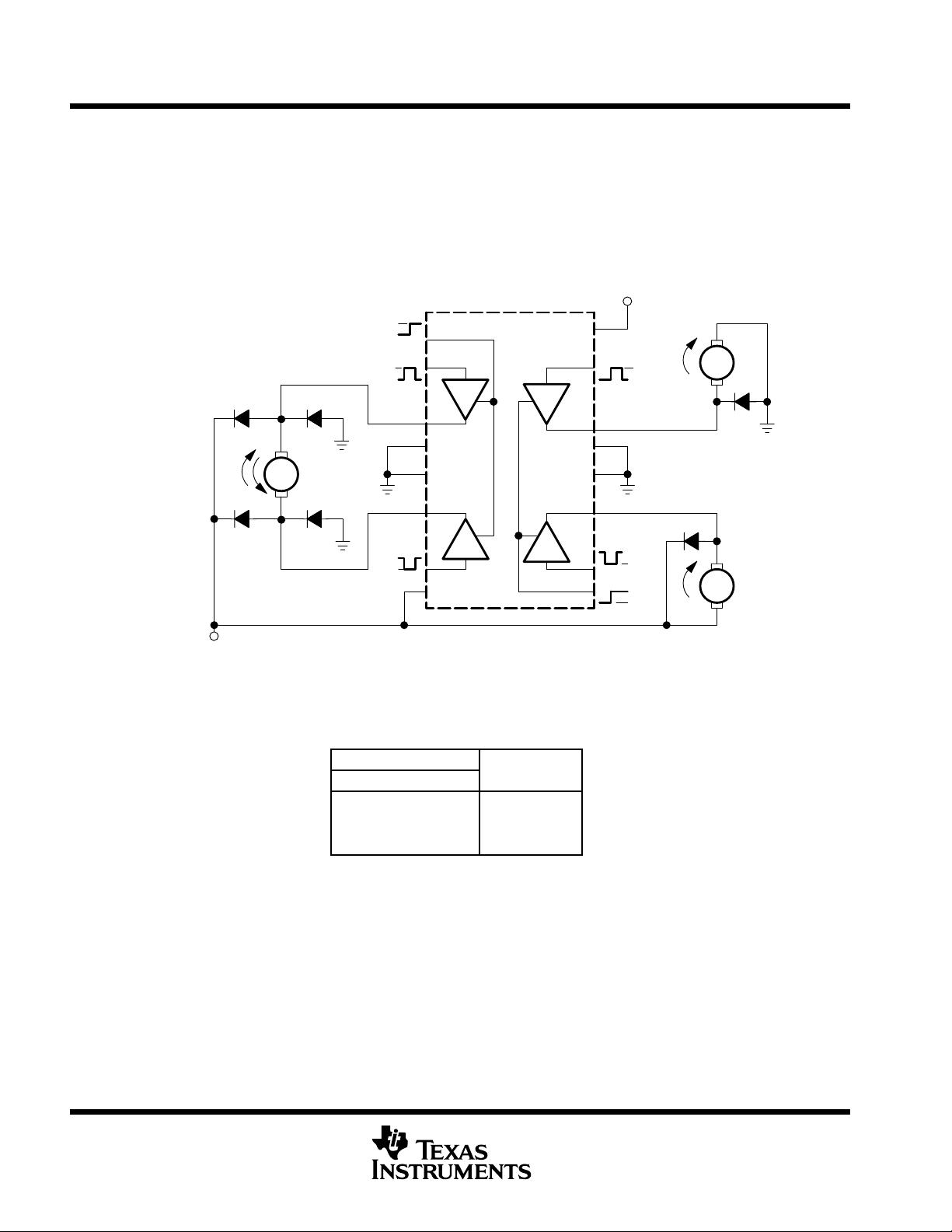
The L293 and L293D are quadruple high-current
half-H drivers. The L293 is designed to provide
bidirectional drive currents of up to 1 A at voltages
from 4.5 V to 36 V. The L293D is designed to
provide bidirectional drive currents of up to
600-mA at voltages from 4.5 V to 36 V. Both
devices are designed to drive inductive loads such
as relays, solenoids, dc and bipolar stepping
motors, as well as other high-current/high-voltage
loads in positive-supply applications.
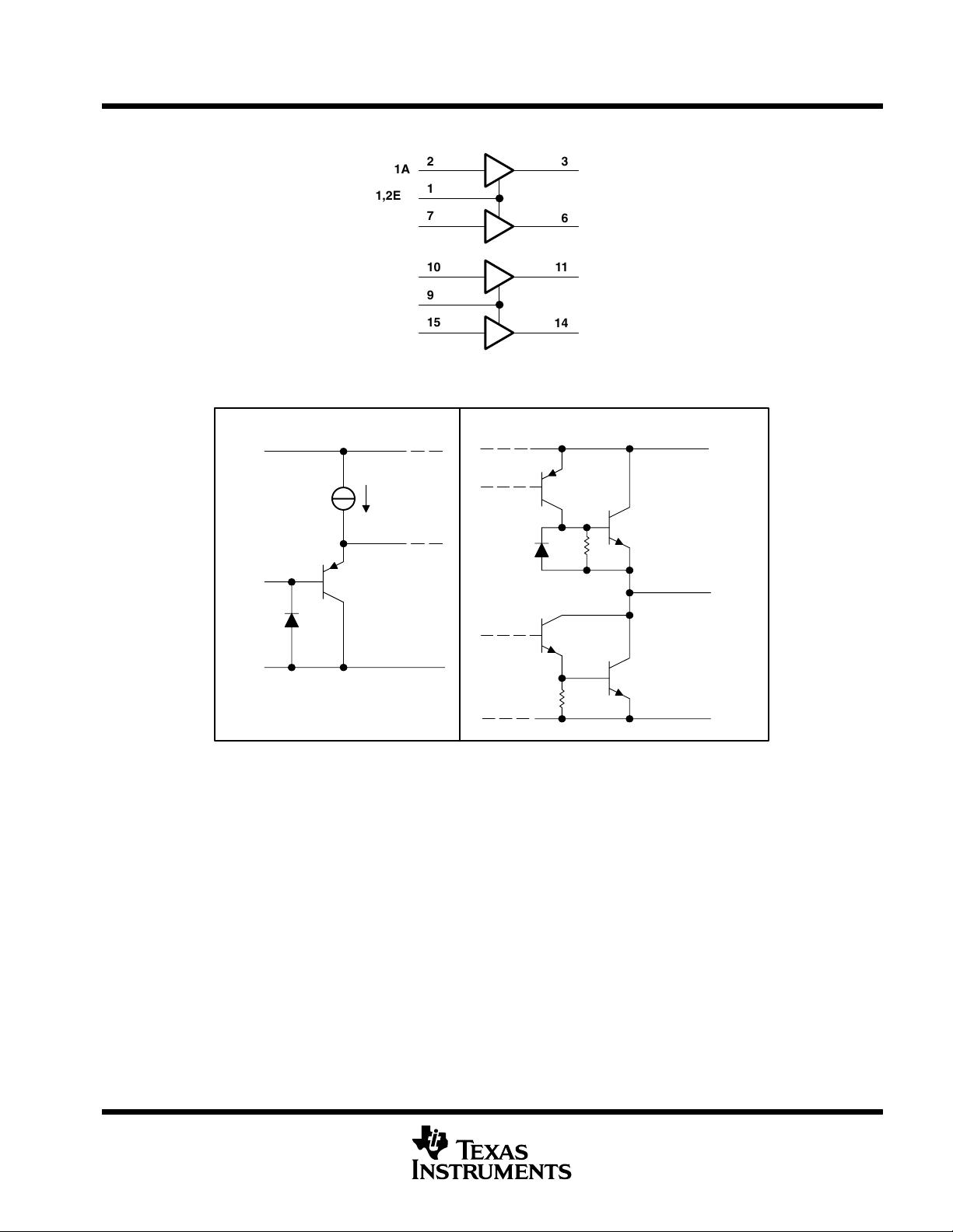
All inputs are TTL compatible. Each output is a
complete totem-pole drive circuit, with a
Darlington transistor sink and a pseudo-
Darlington source. Drivers are enabled in pairs, with drivers 1 and 2 enabled by 1,2EN and drivers 3 and 4
enabled by 3,4EN. When an enable input is high, the associated drivers are enabled, and their outputs are active
and in phase with their inputs. When the enable input is low, those drivers are disabled, and their outputs are
off and in the high-impedance state. With the proper data inputs, each pair of drivers forms a full-H (or bridge)
reversible drive suitable for solenoid or motor applications.
ORDERING INFORMATION
T
A
PACKAGE
†
ORDERABLE
PART NUMBER
TOP-SIDE
MARKING
HSOP (DWP) Tube of 20 L293DWP L293DWP
0°Cto70°C
PDIP (N) Tube of 25 L293N L293N
0°C to 70°C
PDIP (NE)
Tube of 25 L293NE L293NE
PDIP (NE)
Tube of 25 L293DNE L293DNE
†
Package drawings, standard packing quantities, thermal data, symbolization, and PCB design guidelines are available at
www.ti.com/sc/package.
Copyright 2004, Texas Instruments Incorporated
PRODUCTION DATA information is current as of publication date.
Products conform to specifications per the terms of Texas Instruments
standard warranty. Production processing does not necessarily include
testing of all parameters.
Please be aware that an important notice concerning availability, standard warranty, and use in critical applications of
Texas Instruments semiconductor products and disclaimers thereto appears at the end of this data sheet.
HEAT SINK AND
GROUND
HEAT SINK AND
GROUND
1
2
3
4
5
6
7
8
16
15
14
13
12
11
10
9
1,2EN
1A
1Y
2Y
2A
V
CC2
V
CC1
4A
4Y
3Y
3A
3,4EN
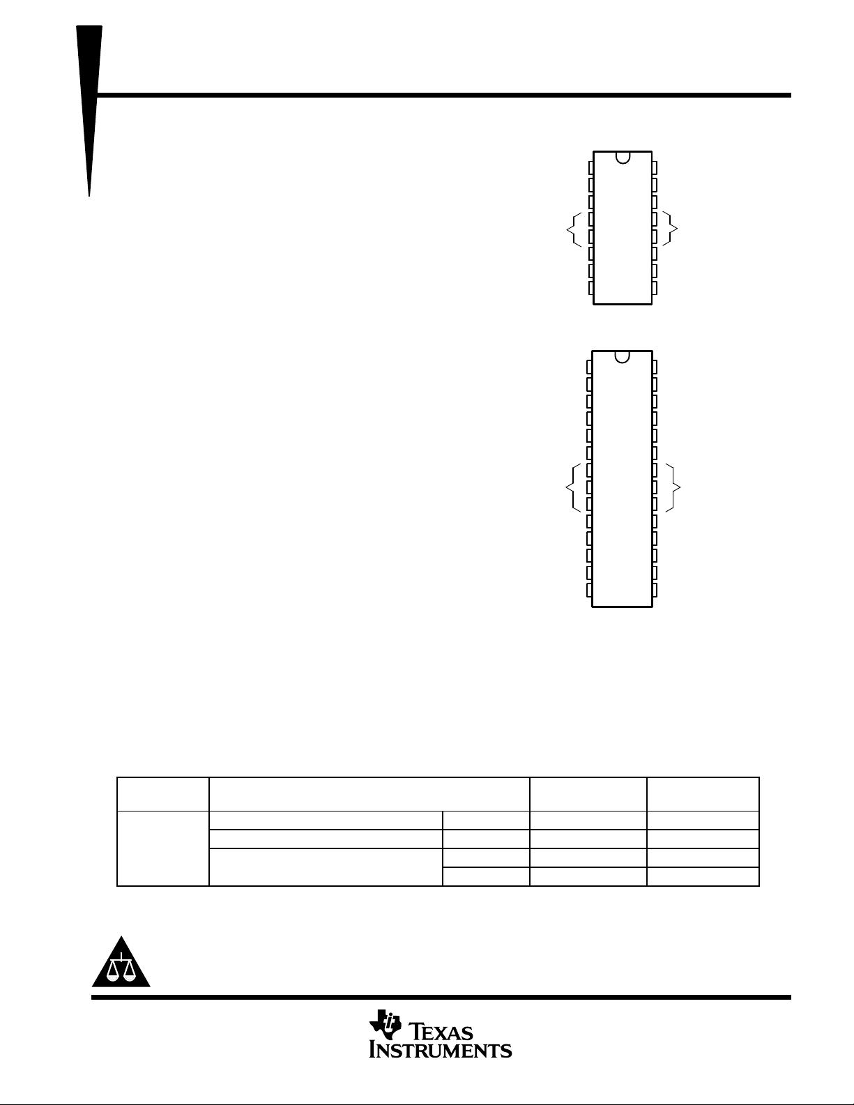
L293 ...N OR NE PACKAGE
L293D . . . NE PACKAGE
(TOP VIEW)
1
2
3
4
5
6
7
8
9
10
11
12
13
14
28
27
26
25
24
23
22
21
20
19
18
17
16
15
1,2EN
1A
1Y
NC
NC
NC
NC
NC
2Y
2A
V
CC2
V
CC1
4A
4Y
NC
NC
NC
NC
NC
3Y
3A
3,4EN
L293 . . . DWP PACKAGE
(TOP VIEW)
HEAT SINK AND
GROUND
HEAT SINK AND
GROUND
剩余16页未读,继续阅读
资源评论


hit_marilyn
- 粉丝: 0
- 资源: 2


最新资源
- C#联合halcon的demo 直线 找圆 形状模板匹配及等级识别等功能 功能有找直线,找圆,形状模板匹配,二维码识别及等级识别,相机内参标定,相机外参标定,以及几何测量 另外还有某论坛的开源控件,并
- BM260、310、410系列.pdf
- P9500系列.pdf
- 西门子PID程序西门子plc模板程序西门子通讯程序案例 1200和多台G120西门子变频器Modbud RTU通讯,带西门子触摸屏,带变频器参数 Modbus通讯报文详细讲解,PID自写FB块无密
- NOI级 数学与其他-2025.01.09(K).pdf
- 毕业设计-基于python大学生就业信息管理系统(django)毕业设计与实现源码+数据库
- 电机控制器,感应异步电机的无传感器矢量控制,完整的C代码+仿真模型: 基于“电压模型+电流模型”的磁链观测器,实现转子磁场定向控制(FOC),可实现电机在低速、中高速段的高精度的转速估算;代码已经成功
- Scrum指南-中文版-2020
- 探索CDN技术:互联网内容加速的分布式解决方案
- Hadoop环境中MapReduce集群的操作命令与Web管理界面介绍
- 西门子PID程序西门子PLC 1200和多台G120西门子变频器Modbud RTU通讯,带西门子触摸屏,带变频器参数 Modbus通讯报文详细讲解,PID自写FB块无密码可以直接应用到程序,PID带
- 大数据处理中PySpark操作与实战案例:RDD创建及基本操作教程
- 毕业设计-基于python招聘数据分析可视化系统(django)毕业设计与实现源码+数据库
- GEE 案例-基于sentinel-2的主成分分析(查看不同波段的主成分结果).pdf
- SUES-大四上-计科课程-学习/考试/复习/实验资料
- 基于分布式驱动电动汽车的车辆状态估计,分别采用无迹卡尔曼,容积卡尔曼,高阶容积卡尔曼观测器等,可估计包括纵向速度,质心侧偏角,横摆角速度,以及四个车轮角速度七个状态 模型中第一个模块是四轮驱动电机
资源上传下载、课程学习等过程中有任何疑问或建议,欢迎提出宝贵意见哦~我们会及时处理!
点击此处反馈


