安森美的NCP4894详细资料
需积分: 10 102 浏览量
2010-11-11
14:01:54
上传
评论
收藏 304KB PDF 举报


© Semiconductor Components Industries, LLC, 2007
January, 2007 − Rev. 9
1 Publication Order Number:
NCP4894/D
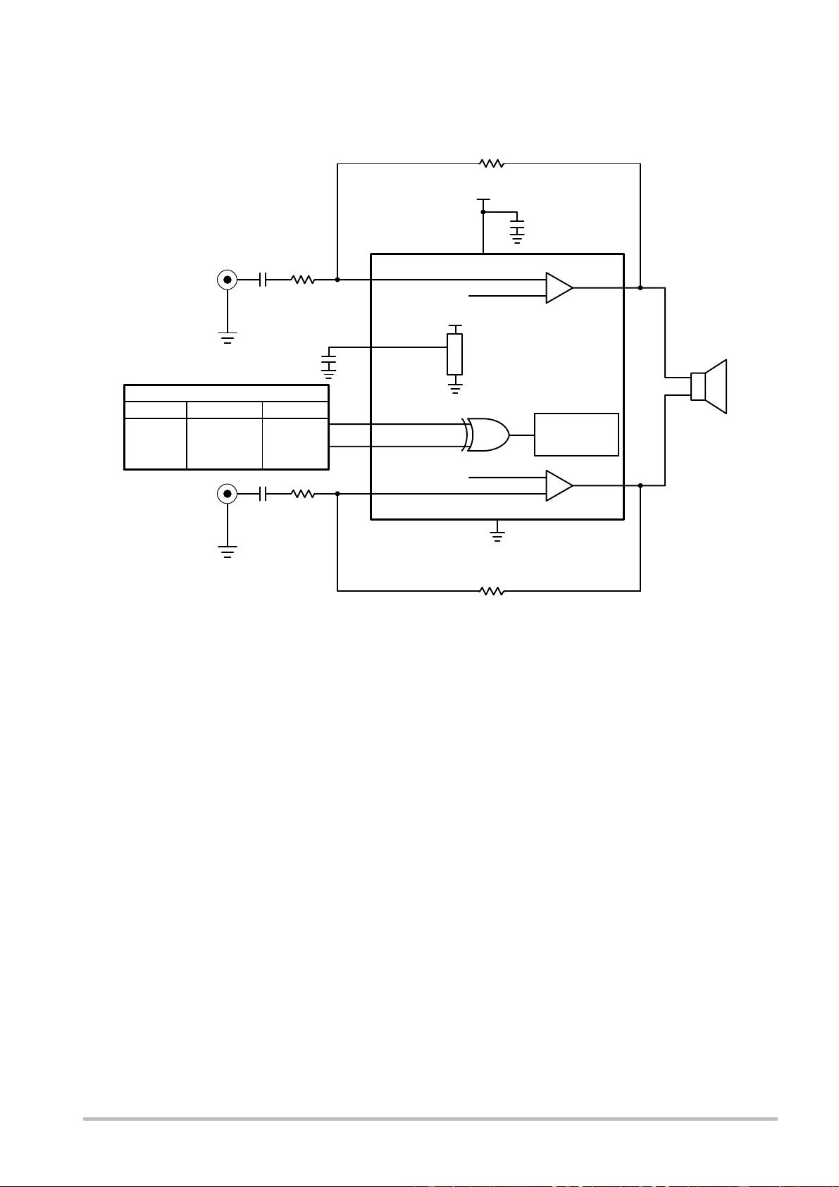
NCP4894
1.8 Watt Differential Audio
Power Amplifier with
Selectable Shutdown
The NCP4894 is a differential audio power amplifier designed for
portable communication device applications. This feature and the
excellent audio characteristics of the NCP4894 are a guarantee of a
high quality sound, for example, in mobile phones applications. With
a 10% THD+N value the NCP4894 is capable of delivering 1.8 W of
continuous average power to an 8.0 W load from a 5.5 V power
supply. With the same load conditions and a 5.0 V battery voltage, it
ensures 1.0 W to be delivered with less than 0.01% distortion.
The NCP4894 provides high quality audio while requiring few
external components and minimal power consumption. It features a
low−power consumption shutdown mode.
To be flexible, shutdown may be enabled by either a logic high or
low depending on the voltage applied on the SD MODE pin.
The NCP4894 contains circuitry to prevent from “pop and click”
noise that would otherwise occur during turn−on and turn−off
transitions.
For maximum flexibility, the NCP4894 provides an externally
controlled gain (with resistors), as well as an externally controlled
turn−on time (with bypass capacitor).
Due to its excellent PSRR, it can be directly connected to the
battery, saving the use of an LDO.
This device is available in 9−Pin Flip−Chip, Micro−10 and DFN10
3x3 mm packages.
Features
• Differential Amplification
• Shutdown High or Low Selectivity
• 1.0 W to an 8.0 W Load from a 5.0 V Power Supply
• Superior PSRR: Direct Connection to the Battery
• “Pop and Click” Noise Protection Circuit
• Ultra Low Current Shutdown Mode
• 2.2 V−5.5 V Operation
• External Gain Configuration Capability
• External Turn−on Configuration Capability
• Thermal Overload Protection Circuitry
• Pb−Free Packages are Available
Typical Applications
• Portable Electronic Devices
• PDAs
• Mobile Phones
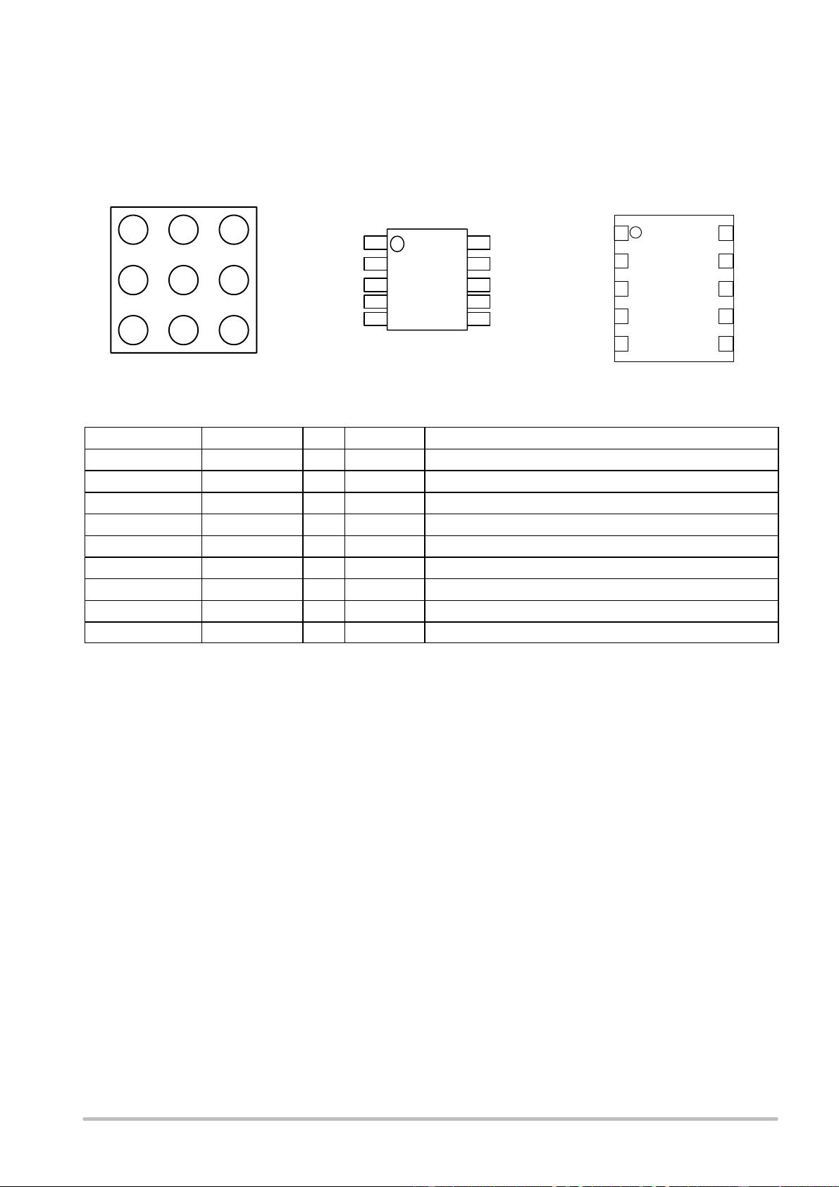
9−PIN FLIP−CHIP
FC SUFFIX
CASE 499AL
http://onsemi.com
xxxx = Specific Device Code
A = Assembly Location
L = Wafer Lot
Y = Year
W, WW = Work Week
G = Pb−Free Package
(Note: Microdot may be in either location)
MARKING
DIAGRAMS
Micro−10
DM SUFFIX
CASE 846B
1
8
1
See detailed ordering and shipping information in the package
dimensions section on page 15 of this data sheet.
ORDERING INFORMATION
xxxG
AYWW
A1
A3
C
1
xxxx
AYWG
G
DFN10
MN SUFFIX
CASE 485C
xxx
ALYWG
G
1
1

剩余19页未读,继续阅读


评论0