没有合适的资源?快使用搜索试试~ 我知道了~
XL1509数据手册.
需积分: 45 12 下载量 111 浏览量
2022-06-20
13:22:04
上传
评论
收藏 2.4MB PDF 举报
温馨提示
试读
12页
XL1509数据手册
资源详情
资源评论
资源推荐
UMW XL1509
Features
n Wide 4.5V to 40V Input Voltage Range
n 3.3V,5V,12V, and adjustable versions
n Output Adjustable from 1.23V to 37V
n Maximum Duty Cycle 100%
n Minimum Drop Out 1.5V
n Fixed 150KHz Switching Frequency
n 3A Constant Output Current Capability
n Internal Optimize Power Transistor
n High efficiency
n Excellent line and load regulation
n TTL shutdown capability
n ON/OFF pin with hysteresis function
n Built in thermal shutdown function
n Built in current limit function
n Built in second current limit function
n Available in SOIC8 package
Applications
n LCD Monitor and LCD TV
n Digital Photo Frame
n Set-up Box
n ADSL Modem
n Telecom / Networking Equipment
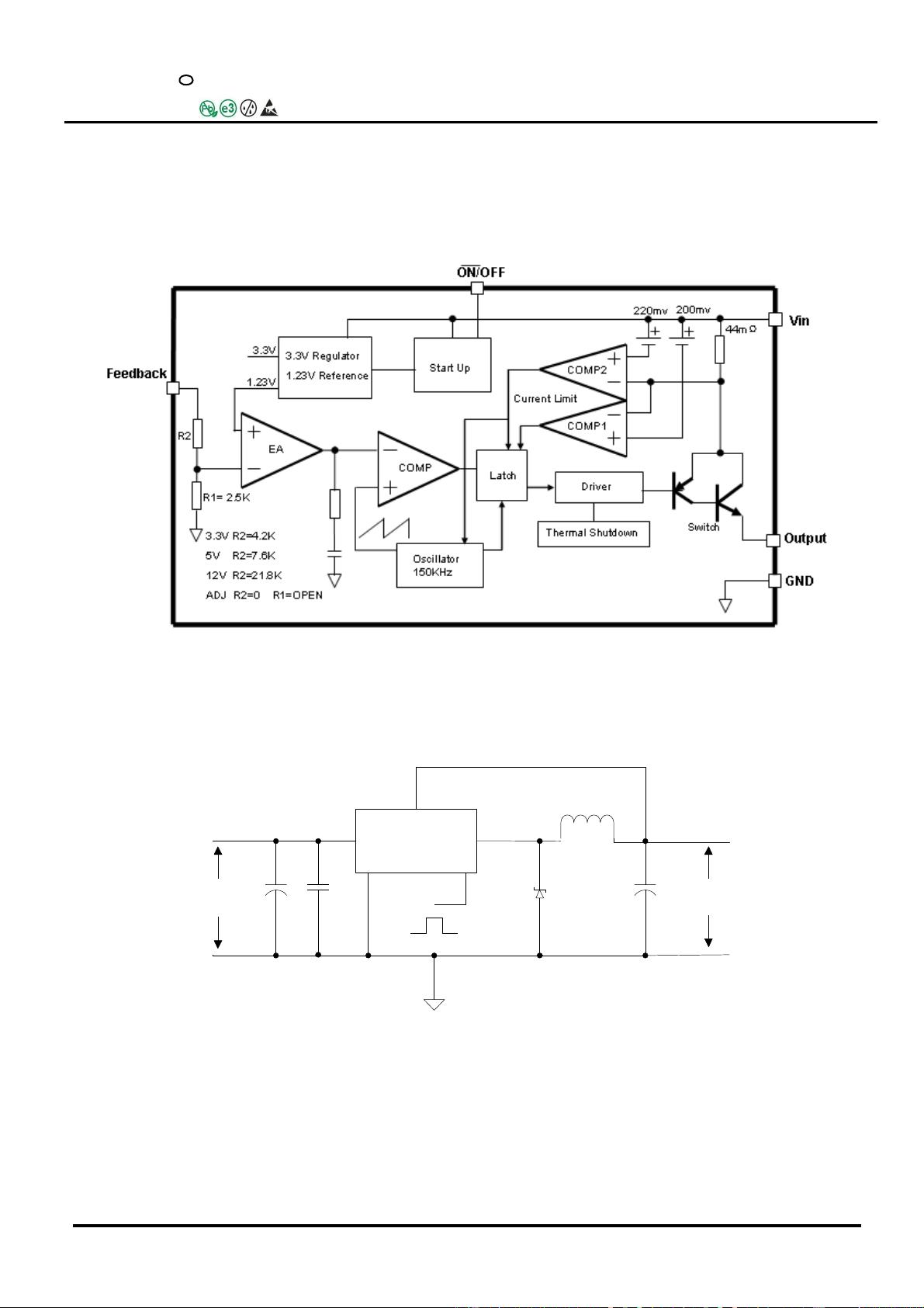
General Description
The XL1509 is a 150 KHz fixed frequency
PWM buck (step-down) DC/DC converter,
capable of driving a 3A load with high
efficiency, low ripple and excellent line and
load regulation. Requiring a minimum
number of external components, the regulator
is simple to use and include internal
frequency compensation and a
fixed-frequency oscillator.
The PWM control circuit is able to adjust the
duty ratio linearly from 0 to 100%. An enable
function, an over current protection function
is built inside. When second current limit
function happens, the operation frequency
will be reduced from 150KHz to 50KHz. An
internal compensation block is built in to
minimize external component count.
Figure1. Package Type of XL1509
UMW
R
UMW XL1509
1
www.umw-ic.com
友台半导体有限公司
2
Pin Configurations
XL1509
1
3
5
2
4 GND
VIN
FEEDBACK
OUTPUT
ON/OFF
6
7
8
GND
GND
GND
Figure2. Pin Configuration of XL1509 (Top View)
Table 1 Pin Description
Pin Number
Pin Name Description
1 VIN
Supply Voltage Input Pin. XL1509 operates from a 4.5V to
40V DC voltage. Bypass Vin to GND with a suitably large
capacitor to eliminate noise on the input.
2 OUTPUT
Power Switch Output Pin (SW). Output is the switch node that
supplies power to the output.
5~8 GND
Ground Pin. Care must be taken in layout. This pin should be
placed outside of the Schottky Diode to output capacitor
ground path to prevent switching current spikes from inducing
voltage noise into XL1509.
3 FEEDBACK
Feedback Pin (FB). Through an external resistor divider
network, Feedback senses the output voltage and regulates it.
The feedback threshold voltage is 1.23V.
4 ON/OFF
Enable Pin. Drive ON/OFF pin low to turn on the device, drive
it high to turn it off. Floating is default low.
UMW XL1509
UMW
R
UMW XL1509
www.umw-ic.com
友台半导体有限公司
3
Function Block
Figure3. Function Block Diagram of XL1509
Typical Application Circuit
XL1509-5.0
CIN C1
105
180uf 35V
D1
L1 68uh/3A
+12V LOAD
1
5~8 4
2
3
GND
VIN
FEEDBACK
OUTPUT
ON/OFF
ON
OFF
5V/3A
COUT
1N5820
470uf 35V
Figure4. XL1509 Typical Application Circuit 12V-5V/3A
UMW XL1509
UMW
R
UMW XL1509
www.umw-ic.com
友台半导体有限公司
剩余11页未读,继续阅读
gushu114122
- 粉丝: 0
- 资源: 73
上传资源 快速赚钱
- 我的内容管理 展开
- 我的资源 快来上传第一个资源
- 我的收益 登录查看自己的收益
- 我的积分 登录查看自己的积分
- 我的C币 登录后查看C币余额
- 我的收藏
- 我的下载
- 下载帮助
安全验证
文档复制为VIP权益,开通VIP直接复制
信息提交成功
评论0