没有合适的资源?快使用搜索试试~ 我知道了~
24AA02UID/24AA025UID数据手册
需积分: 5 0 下载量 24 浏览量
2022-05-13
12:42:01
上传
评论
收藏 612KB PDF 举报
温馨提示
试读
30页
24AA02UID/24AA025UID数据手册
资源详情
资源评论
资源推荐
2013 Microchip Technology Inc. DS20005202A-page 1
24AA02UID/24AA025UID
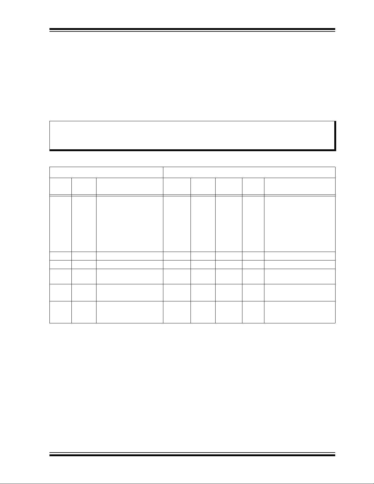
Device Selection Table
Features:
• Preprogrammed 32-Bit Serial Number:
- Unique across all UID-family EEPROMs
- Scalable to 48-bit, 64-bit, 128-bit, 256-bit,
and other lengths
• Single Supply with Operation Down to 1.7V
• Low-Power CMOS Technology:
- Read current 1 mA, max.
- Standby current 1 A, max.
• 2-Wire Serial Interface, I
2
C™ Compatible
• Schmitt Trigger Inputs for Noise Suppression
• Output Slope Control to Eliminate Ground Bounce
• 100 kHz and 400 kHz Clock Compatibility
• Page Write Time 3 ms, typical
• Self-Timed Erase/Write Cycle
• Page Write Buffer:
- 8-byte page (24AA02UID)
- 16-byte page (24AA025UID)
• ESD Protection >4,000V
• More than 1 Million Erase/Write Cycles
• Data Retention >200 Years
• Factory Programming Available
• Available Packages:
- 8-lead PDIP, 8-lead SOIC, and 5-lead
SOT-23 (24AA02UID)
- 8-lead PDIP, 8-lead SOIC, and 6-lead
SOT-23 (24AA025UID)
• RoHS Compliant
• Temperature Ranges:
- Industrial (I): -40°C to +85°C
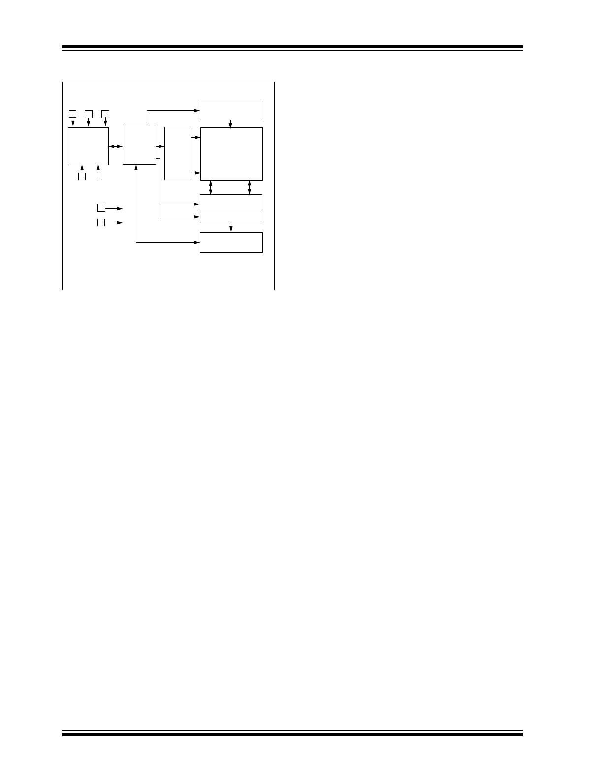
Description:
The Microchip Technology Inc. 24AA02UID/
24AA025UID (24AA02XUID*) is a 2 Kbit Electrically
Erasable PROM with a preprogrammed, 32-bit
unique ID. The device is organized as two blocks of
128 x 8-bit memory with a 2-wire serial interface.
Low-voltage design permits operation down to 1.7V,
with maximum standby and active currents of only
1 A and 1 mA, respectively. The 24AA02XUID also
has a page write capability for up to eight bytes of
data (16 bytes on the 24AA025UID). The
24AA02XUID is available in the standard 8-pin PDIP,
8-pin SOIC, 5-lead SOT-23, and 6-lead SOT-23
packages.
Package Types (24AA02UID)
Package Types (24AA025UID)
Part Number
VCC
Range
Max. Clock
Frequency
Temp.
Ranges
Cascadable Page Size
Unique ID
Length
24AA02UID 1.7-5.5V 400 kHz
(1)
INo8-Byte32-Bit
24AA025UID 1.7-5.5V 400 kHz
(1)
I Yes 16-Byte 32-Bit
Note 1: 100 kHz for VCC <2.5V
PDIP/SOIC
NC
NC
NC
V
SS
1
2
3
4
8
7
6
5
V
CC
NC
SCL
SDA
SOT-23
15
43
SCL
Vss
SDA
NC
Vcc
2
PDIP/SOIC
A0
A1
A2
V
SS
1
2
3
4
8
7
6
5
V
CC
NC
SCL
SDA
SOT-23
V
CC
SCL
SDA
V
SS
A0
A1
1
2
3
4
5
6
2K I
2
C™ Serial EEPROMs with Unique 32-bit Serial Number
*24AA02XUID is used in this document as a generic
part number for the 24AA02UID/24AA025UID devices.
24AA02UID/24AA025UID
DS20005202A-page 2 2013 Microchip Technology Inc.
Block Diagram
I/O
Control
Logic
Memory
Control
Logic XDEC
HV Generator
EEPROM
Array
Write-Protect
Circuitry
YDEC
V
CC
VSS
SDA
SCL
Note 1: Pins A0, A1 and A2 are not available on
the 24AA02UID.
A0
(1)
A1
(1)
A2
(1)
Sense Amp.
R/W Control
2013 Microchip Technology Inc. DS20005202A-page 3
24AA02UID/24AA025UID
1.0 ELECTRICAL CHARACTERISTICS
Absolute Maximum Ratings
(†)
VCC.............................................................................................................................................................................6.5V
All inputs and outputs w.r.t. V
SS ..........................................................................................................-0.3V to VCC +1.0V
Storage temperature ...............................................................................................................................-65°C to +150°C
Ambient temperature with power applied..................................................................................................-40°C to +85°C
ESD protection on all pins 4kV
TABLE 1-1: DC CHARACTERISTICS
† NOTICE: Stresses above those listed under “Absolute Maximum Ratings” may cause permanent damage to the
device. This is a stress rating only and functional operation of the device at those or any other conditions above those
indicated in the operational listings of this specification is not implied. Exposure to maximum rating conditions for
extended periods may affect device reliability.
DC CHARACTERISTICS
Industrial (I): T
A = -40°C to +85°C, VCC = +1.7V to +5.5V
Param.
No.
Sym. Characteristic Min. Typ. Max. Units Conditions
— SCL, SDA, A0, A1, and
A2 pins
— ————
D1 V
IH High-level Input Voltage 0.7 VCC ——V—
D2 VIL Low-level Input Voltage — — 0.3 VCC V—
D3 VHYS Hysteresis of Schmitt
Trigger inputs
0.05 VCC ——V(Note)
D4 V
OL Low-level Output Voltage — — 0.40 V IOL = 3.0 mA, VCC = 2.5V
D5 ILI Input Leakage Current ——±1AVIN = VSS or VCC
D6 ILO Output Leakage Current ——±1AVOUT = VSS or VCC
D7 CIN,
C
OUT
Pin Capacitance
(all inputs/outputs)
——10pFVCC = 5.0V (Note)
T
A = 25°C, FCLK = 1 MHz
D8 I
CC write Operating Current —0.1 3mAVCC = 5.5V, SCL = 400 kHz
D9 ICC read — 0.05 1 mA —
D10 ICCS Standby Current —0.01 1 Industrial
SDA = SCL = V
CC
A0, A1, A2 = VSS
Note: This parameter is periodically sampled and not 100% tested.
24AA02UID/24AA025UID
DS20005202A-page 4 2013 Microchip Technology Inc.
TABLE 1-2: AC CHARACTERISTICS
AC CHARACTERISTICS
Industrial (I): T
A = -40°C to +85°C, VCC = +1.7V to +5.5V
Param.
No.
Sym. Characteristic Min. Typ. Max. Units Conditions
1F
CLK Clock frequency —
—
—
—
400
100
kHz 2.5V VCC 5.5V
1.7V V
CC 2.5V
2 THIGH Clock high time 600
4000
—
—
—
—
ns 2.5V VCC 5.5V
1.7V V
CC 2.5V
3TLOW Clock low time 1300
4700
—
—
—
—
ns 2.5V VCC 5.5V
1.7V V
CC 2.5V
4T
R SDA and SCL rise time
(Note 1)
—
—
—
—
300
1000
ns 2.5V VCC 5.5V (Note 1)
1.7V V
CC 2.5V (Note 1)
5TF SDA and SCL fall time — —
—
300 ns (Note 1)
6T
HD:STA Start condition hold time 600
4000
—
—
—
—
ns 2.5V VCC 5.5V
1.7V V
CC 2.5V
7T
SU:STA Start condition setup
time
600
4700
—
—
—
—
ns 2.5V VCC 5.5V
1.7V V
CC 2.5V
8THD:DAT Data input hold time 0 —
—
—ns(Note 2)
9T
SU:DAT Data input setup time 100
250
—
—
—
—
ns 2.5V VCC 5.5V
1.7V V
CC 2.5V
10 T
SU:STO Stop condition setup
time
600
4000
—
—
—
—
ns 2.5V VCC 5.5V
1.7V V
CC 2.5V
11 TAA Output valid from clock
(Note 2)
—
—
—
—
900
3500
ns 2.5V VCC 5.5V
1.7V V
CC 2.5V
12 TBUF Bus free time: Time the
bus must be free before
a new transmission can
start
1300
4700
—
—
—
—
ns 2.5V VCC 5.5V
1.7V V
CC 2.5V
13 TOF Output fall time from VIH
minimum to V
IL
maximum
—
—
—
—
250
250
ns 2.5V V
CC 5.5V
1.7V V
CC 2.5V
14 T
SP Input filter spike
suppression
(SDA and SCL pins)
— — 50 ns (Notes 1 and 3)
15 TWC Write cycle time (byte or
page)
——5ms—
16 — Endurance 1M — — cycles 25°C (Note 4)
Note 1: Not 100% tested. C
B = total capacitance of one bus line in pF.
2: As a transmitter, the device must provide an internal minimum delay time to bridge the undefined region
(minimum 300 ns) of the falling edge of SCL to avoid unintended generation of Start or Stop conditions.
3: The combined T
SP and VHYS specifications are due to new Schmitt Trigger inputs which provide improved
noise spike suppression. This eliminates the need for a
TI specification for standard operation.
4: This parameter is not tested but ensured by characterization. For endurance estimates in a specific
application, please consult the Total Endurance™ Model which can be obtained from Microchip’s web site
at www.microchip.com.
2013 Microchip Technology Inc. DS20005202A-page 5
24AA02UID/24AA025UID
FIGURE 1-1: BUS TIMING DATA
FIGURE 1-2: BUS TIMING START/STOP
7
5
2
4
8
9
10
12
11
14
6
SCL
SDA
IN
SDA
OUT
3
7
6
D3
10
Start Stop
SCL
SDA
剩余29页未读,继续阅读
gushu114122
- 粉丝: 0
- 资源: 73
上传资源 快速赚钱
- 我的内容管理 展开
- 我的资源 快来上传第一个资源
- 我的收益 登录查看自己的收益
- 我的积分 登录查看自己的积分
- 我的C币 登录后查看C币余额
- 我的收藏
- 我的下载
- 下载帮助
安全验证
文档复制为VIP权益,开通VIP直接复制
信息提交成功
评论0