没有合适的资源?快使用搜索试试~ 我知道了~
资源推荐
资源详情
资源评论

1-1
Understanding and Optimizing Electromagnetic
Compatibility in Switchmode Power Supplies
Bob Mammano and Bruce Carsten
A
BSTRACT
Electromagnetic noise issues have long been a concern with switching power supplies, as their high-
frequency switching of voltage and current generate higher order harmonics that have the potential to
cause interference with system operation. While international specifications and standardized testing
procedures have at least provided a greater understanding of the problems, optimum solutions must still
come from techniques that are applied during the design process. This topic attempts to describe the
more significant causes of EMI in power supplies and offer design techniques to minimize their impact.
I.
I
NTRODUCTION
While switchmode power supplies are well
known and appreciated for their significant
benefits in reductions to both physical size and
internal power loss, the threat of generating
electromagnetic interference (EMI) from the high
frequencies inherent in their fast-changing
voltage and current waveforms has always been a
serious concern. As advances in power supply
technology have increased switching frequencies,
and allowed these supplies to be used in closer
proximity to the systems they power, these
concerns – and the demands that designers react
to them – have only heightened. Thus, designing
for electromagnetic compatibility (EMC) has
become a requirement every bit as important as
meeting a given set of power conversion
performance specifications, and it is the purpose
of this discussion to address some of the more
important principles and techniques involved.
First, note that while we have used the terms
EMI and EMC interchangeably, it should be clear
that one is the inverse of the other. The accepted
definition of EMI is: the interference of one piece
of electronic equipment on the operation of
another by means of electromagnetic energy
transfer.
And electromagnetic compatibility (EMC) is
the absence of EMI. Two things follow from this
definition. The first is that EMC is a system-level
consideration. While it is common to test for
electromagnetic noise generation from a power
supply as a stand-alone box, the ultimate
standards that have to be met apply to the system
as a whole with the power supply as an internal
component or subsystem. And the second aspect
of this definition of EMI is that it involves three
elements:
• A generator of electromagnetic energy:
(a source).
• Transmission of that energy between
equipments: (a coupling means).
• A receptor circuit whose operation is
negatively impacted by the transmitted
energy: (a victim circuit).
All three elements must be present for EMI to
take place – remove any one and there can be no
interference. However, while shielding or
separation may solve a specific interference
problem by attacking the coupling or
susceptibility part of the system, the preferable
approach is to remove the problem at the source –
and that will be the thrust of this discussion.

1-2
II.
U
NDERSTANDING
EMI
While it may at times seem otherwise, EMI is
not a black art. Although often neglected in basic
circuit design education, and appearing
sometimes to be quite complex in practice, the
basic principles for both causing and correcting
EMI are relatively simple. Fundamentally, it
requires a recognition of the fields caused by
rapidly changing currents and voltages. While
these characteristics are quantitatively described
by Maxwell’s equations, we need only to know
that electronic noise may be induced by coupling
between circuit elements through the action of
either a magnetic or an electric field.
A magnetic field will cause a changing
current in a conductor to induce a voltage in
another according to:
dtdiMe •=
where M is the mutual inductance between
the source and the victim.
Similarly, an electric field will cause a
changing voltage on a surface to induce a current
to flow in another conductor according to:
dtdvCi •=
where C is the capacitance coupling the
source to the victim.
These equations tell us that where we have
rapidly changing currents – as in the conductors
in series with power switching devices – we can
expect to see an induced voltage across other
conductors coupled by a mutual inductance. And
where there is a high dv/dt – as on the drain
contacts of the power switching FETs – any
parasitic capacitance can couple an induced
current into another path. While it may not be
very helpful, it should probably be noted that one
of the most obvious ways to reduce generated
EMI would be to slow down the switching
transitions, but the cost in increased switching
losses typically makes this a less viable solution.
One important point to keep in mind on this
subject is that EMI is a very low energy
phenomenon! Because it can take an extremely
small amount of energy, induced at the right
place in the victim, to upset system performance,
noise specification limits have been established at
very small values. For example, at 1 MHz, it
takes only 20 nW of measured EMI power to fail
FCC requirements. This could be experienced
with energy coupling of just a few parts per
billion. Thus an easy trap to fall into is to
discount some possible noise sources as too
insignificant to be worth considering.
III.
M
EASURING
EMI
When we describe a potential noise-
generating system, the transmission of the noise
out of the system is by either or both of two
separate coupling paths: as radiated energy from
the system itself by way of magnetic or electric
fields (as described above), or as conducted
energy flowing in either the input, output, or
control lines connecting the system under
evaluation to the “rest-of-the-world”, where these
lines can then become secondary radiators. These
conducting and radiating EMI noise sources are
considered as separate and distinct and are
typically specified separately when evaluating the
external characteristics of a definable system.
One helpful characteristic, however, is that the
efficiency of noise coupling is frequency
dependent - the higher the frequency, the greater
the potential for radiated EMI, while at lower
frequencies, problems are more likely to be
caused by conducted noise. There seems to be
universal agreement that 30 MHz is the crossover
frequency between conducted and radiated EMI.
Most regulating agencies throughout the world
have thus established measurement standards
specifying the evaluation of conducted
EMI at
frequencies up to 30 MHz, with a separate set of
standards applicable above 30 MHz for radiated
EMI. We will discuss these two types of noise
sources separately, but before doing so, some
additional comparative information might be
helpful.

1-3
Conducted noise is primarily driven by
current but is measured as a noise voltage by
using a 50-Ω current shunt. Moreover, with our
discussion herein limited to power supplies, the
FCC position is that only the ac input power lines
are of concern, since it is here where noise
currents could most readily couple to other
systems through the power distribution network.
While the maximum frequency of interest for
conducted noise is 30 MHz, the minimum
frequency limit can vary. In the United States and
Canada, that limit is usually 450 kHz but many
international specifications place the lower limit
at 150 kHz. And some telecom specs require
testing all the way down to 10 kHz.
With radiated noise specifications starting
with a lower limit of 30 MHz, the upper limits
can range from a few hundred MHz to 1 GHz or
more. And while conducted noise can be
evaluated with not much more laboratory
equipment than a spectrum analyzer and a
coupling device, radiated noise requires the
measurement of magnetic or electric fields in free
space, causing the testing to become much more
complex. For this reason, radiation testing is
usually performed by a separate, specialized test
facility, where variables inherent in the testing
environment may be very closely defined and
controlled.
And speaking of variables, a non-trivial
decision that needs to be made right at the
beginning, is which specification to use. We have
already alluded to the fact that each country has
its own set of specifications for EMI, but within
this distinction, there are additional determinates
defined by product type and usage. For example,
some specs define power supplies as “digital
devices” while others combine them with
“information technology” specifications. System
usage also defines “Classes” where Class A
designates industrial and commercial
applications, and Class B includes residential
usage. Class B limits are typically more stringent
under the assumptions that systems made for the
home are likely to be in closer proximity, and
that residential users typically have fewer options
available for dealing with EMI.
In the United States, the Federal
Communications Commission (FCC) owns the
responsibility for the control of electromagnetic
interference through the Code of the Federal
Register (CFR), Title 47. Within this document,
Part 15 controls Information Technology
Equipment (ITE), Part 18 covers Industrial,
Scientific and Medical Equipment (ISM), and
Part 68 regulates equipment connected to a
telephone network.
International EMI specifications have been
led by the International Electrotechnical
Commission (IEC), which has published a
European Union generic standard for emissions
(EN50081), and the French-led Comité
International Spécial des Perturbations
Radioélectriques (CISPR). This latter body has
issued their specification - CISPR Publication 22
- which is gaining world-wide acceptance and, in
so doing, is applying pressure for FCC
acceptance of the same standards.
At the time of this writing, noteworthy
differences between the FCC and CISPR
specifications include, in addition to some limit
value differences, a lower frequency range for
CISPR conducted noise measurements, and
radiation tests made at a fixed distance of 10
meters vs 3 to 30 meters for FCC testing. By
extrapolating the FCC radiation limits to 10
meters (linearly proportional to 1/distance) the
comparisons can be better illustrated with the
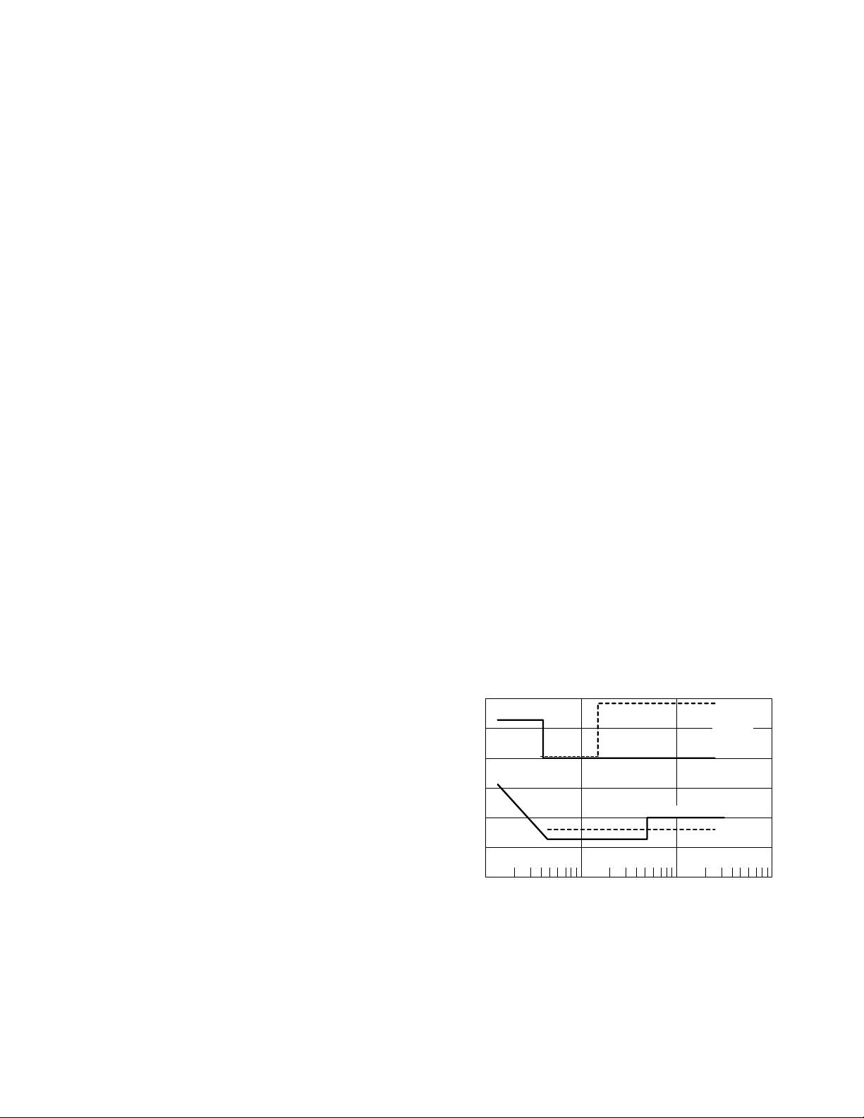
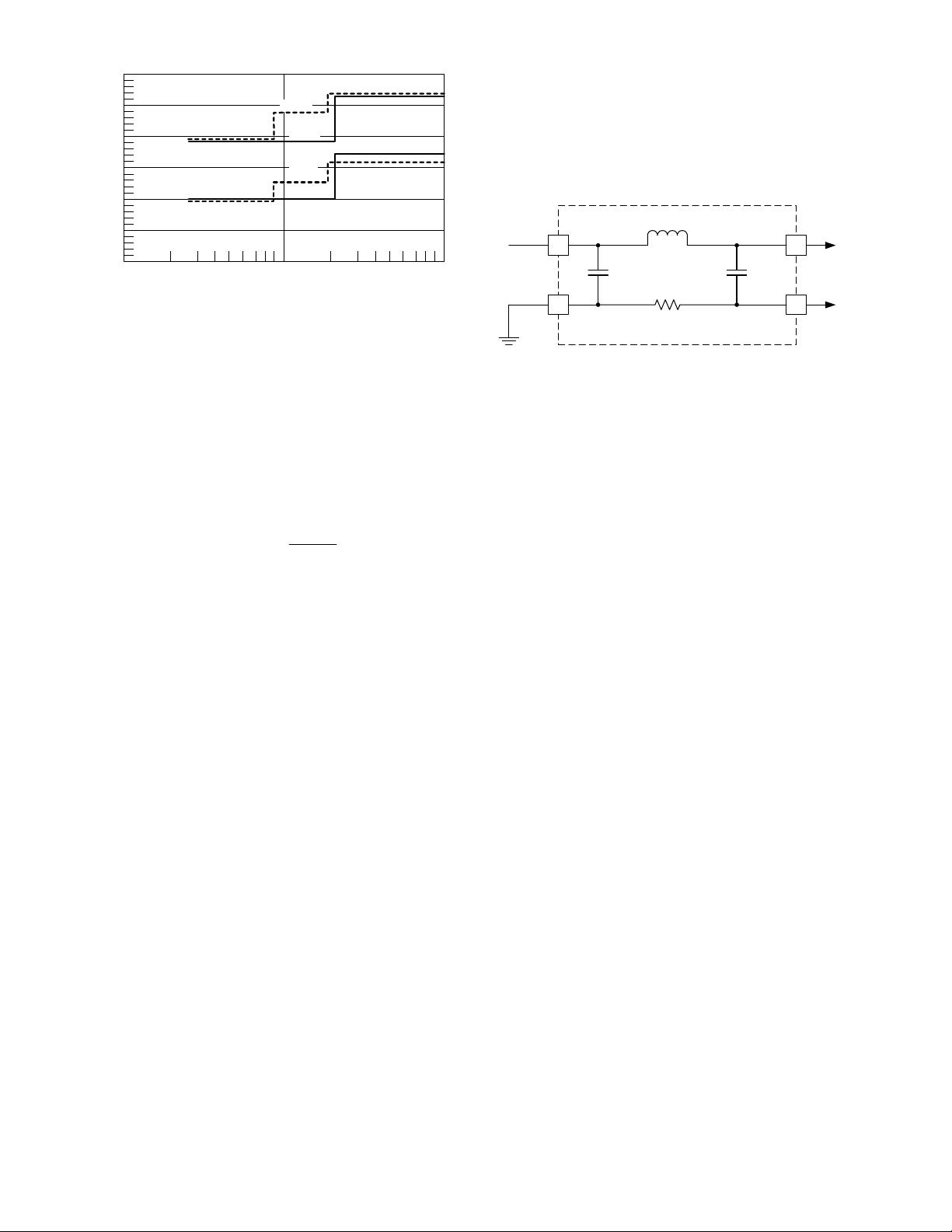
frequency plots shown in Figs. 1 and 2.
[Ref. 2]
70
65
60
55
50
45
40
Frequency - MHz
Voltage - dBµV
0.1 0.3 0.50.2
FCC
FCC
CISPR
CLASS B
CLASS A
135102 30 50 10020
CISPR
Fig. 1. Conducted noise limits,
(FCC Part 15 vs. CISPR 22).

1-4
50
45
40
35
30
25
20
10 30 50 100 500 1000
Frequency - MHz
Field Strength - dB
µV/m
30020020
FCC
CISPR
CISPRCLASS B
CLASS A
Measuring Distance = 10 m
FCC
Fig. 2. Radiated noise limits,
(FCC Part 15 vs. CISPR 22).
Note that the units in these specifications are
given as dBµV for direct measurements of
conducted noise and dBµV/m for field strength
measurements of radiated noise as sensed with an
antenna. These are decibel values giving the ratio
between the actual voltage measurement and one
microvolt. The calculation is:
µ
=µ
V0.1
V
log20VdB
10
and it applies to both volts and volts/meter.
Finally, with all the variables we have been
discussing, we have not mentioned one that you
might consider quite important - the operating
conditions of the equipment under test. The
reason is that this raises so many other questions
that it defies definition. For example, do you test
at the highest input voltage where dV/dt will
likely be at a peak, or at the lowest voltage,
maximum load where dI/dt will probably be
highest? And in the power circuitry, there is one
current path when the power switch is on and
another when it is off, so duty cycle is likely to
be a variable. As a result, in most cases the
operating conditions are left to whatever the
manufacturer defines as “typical” but suppliers
should recognize this as a potential issue in
correlating data.
IV.
C
ONDUCTED
EMI
We now will delve more specifically into the
causes and design implications of each of the two
major categories of EMI, focusing initially on
conducted noise as measured on the power
supply’s input power feed lines. To observe
conducted noise on a power line, a device is
needed to separate the high-frequency noise
signals from the input current, and that device is
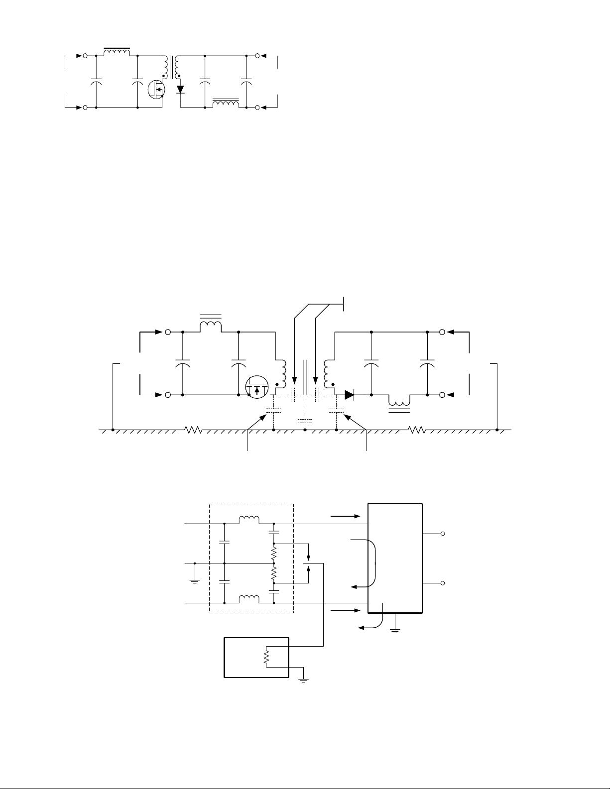
called a Line Impedance Stabilization Network,
or LISN, and shown schematically in Fig. 3.
10 µF
10 nF
to
330 nF*
50 Ω
50 µH
Power
Source
Ground
Power
Supply
Input
To
Spectrum
Analyzer
LISN
* Capacitor value determined by lowest
specified frequency.
Fig. 3. A 120/240 VAC, 60 Hz LISN circuit. All
measurements are made with respect to ground.
This device allows the use of a spectrum
analyzer to measure the noise current through a
50-Ω source impedance while isolating the
measurement from any high-frequency shunting
which might exist in the power distribution
network. Typically, a LISN network is added to
each of the input power lines and the noise
signals are measured with respect to ground.
Conducted noise at the power supply’s input
can be further sub-categorized into two separate
modes of current flow: differential mode (DM)
noise, as measured between the power feed and
its return path; and common mode (CM) noise
which is measured between each of the power
lines and ground. The contributors to these two
modes are inherent to the basic operation of a
switching power supply. The action of the
internal power switches causes rapid dI/dt
changes in the differential current at both the
input and outputs of the power supply, as
illustrated in Fig. 4. Of course, input and output
filters ideally would eliminate any high
frequency noise external to the power supply, but
neither can do the job completely. So residual
ripple and switching spikes exist as a differential
mode noise source with current flow
bidirectionally into one terminal and out the
other.

1-5
INPUT
NOISE
OUTPUT
NOISE
Fig. 4. Differential mode (DM) noise current is
produced by normal switching action.
There are also sources of rapidly changing
voltage within the power supply which can
couple noise through parasitic capacitance to
earth ground, some of which are shown in Fig. 5.
This type of noise in the ground path, which can
be seen as common mode noise on all power
supply terminals, is measured with respect to
ground.
The paths for both DM and CM noise
currents at the power supply’s input are shown in
very simplified form in Fig. 6, which also shows
the application of two LISN devices, in series
with both the power line input and its return.
Note that both CM and DM modes of current
are present in each LISN but, with the polarities
shown, the power line LISN measures CM +
DM, while the LISN on the neutral return
measures CM – DM. Both of these quantities are
vector sums and, where necessary, there are
circuit networks that can be used to separate CM
and DM signals,
[Ref. 9]
but the specifications
typically do not differentiate. The total noise at
each input must be measured because, with the
possibility of multiple current paths within the
power supply, there is no reason to assume that
the values of the CM and DM contributions at the
two inputs are identical.
Input
Noise
Output
Noise
Capacitive Currents Direct to Chassis
Capacitive Currents Primary
to Secondary
Chassis Ground Chassis Ground Chassis Ground
Fig. 5. Common mode (CM) noise occurs when transients from switching voltages are coupled to earth
(or chassis) ground through parasitic capacitances.
Two LISN Circuits
Spectrum
Analyzer
50 Ω
SMPS
DM
OUTPUTS
CM
CM
CM
NEUTRAL
GROUND
LINE
CM and DM add vectorially
EMI (line) = CM + DM
EMI (neutral) = CM - DM
Fig. 6. DM and CM currents at the power supply’s input.
剩余175页未读,继续阅读
资源评论

 jiewoyimoxiao2014-06-27还是不错的
grfly
- 粉丝: 1
- 资源: 12
上传资源 快速赚钱
 我的内容管理
展开
 我的资源
快来上传第一个资源
 我的收益 登录查看自己的收益
 我的积分
登录查看自己的积分
 我的C币
登录后查看C币余额
 我的收藏
我的收藏  我的下载
我的下载  下载帮助
下载帮助

 前往需求广场,查看用户热搜
最新资源
资源上传下载、课程学习等过程中有任何疑问或建议,欢迎提出宝贵意见哦~我们会及时处理!
点击此处反馈


安全验证
文档复制为VIP权益,开通VIP直接复制
 信息提交成功