ASIC牛人之经典总结


Typical ASIC design flow .................................................................................................................2
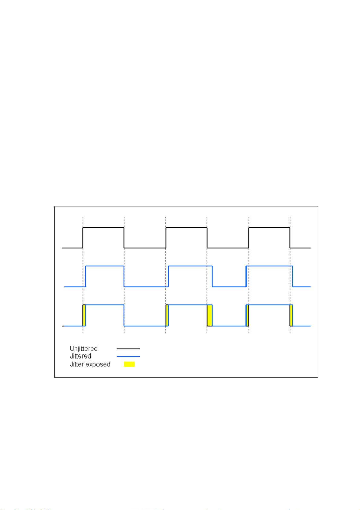
时钟抖动 (Clock Jitter) ....................................................................................................................5
信号同步的窍门...............................................................................................................................8
数字后端流程...................................................................................................................................9
DC 概论之一 setup time 与 hold time .......................................................................................11
DC 概论二之 fanout 与 skew.........................................................................................................14
DC 概论三之 setup time 与 hold time 之二................................................................................21
DC 概论四之 setup time 与 hold time 之三.................................................................................26
DC 概论五之 high fanout...............................................................................................................42
DC 概论六之 multicycle_path ......................................................................................................58
DC 概论七之 gated clock...............................................................................................................75
DC 概论之 IO 约束........................................................................................................................84
DC 优化约束 ..................................................................................................................................90
Synopsys Synthesis Constraints Template ......................................................................................92
功耗和门控时钟的的基本概念.....................................................................................................95
对 FALSE PATH 的理解 ................................................................................................................97
TimeQuest 时钟分析....................................................................................................................101
静态时序分析...............................................................................................................................105
寄生参数提取和静态时序分析...................................................................................................124
IC 设计中的时钟类型约束..........................................................................................................130
IC 设计流程及工具......................................................................................................................132


剩余133页未读,继续阅读


评论2
最新资源