© Semiconductor Components Industries, LLC, 2019
August, 2019 − Rev. 0
1 Publication Order Number:
NTMFS5C628N/D
NTMFS5C628N
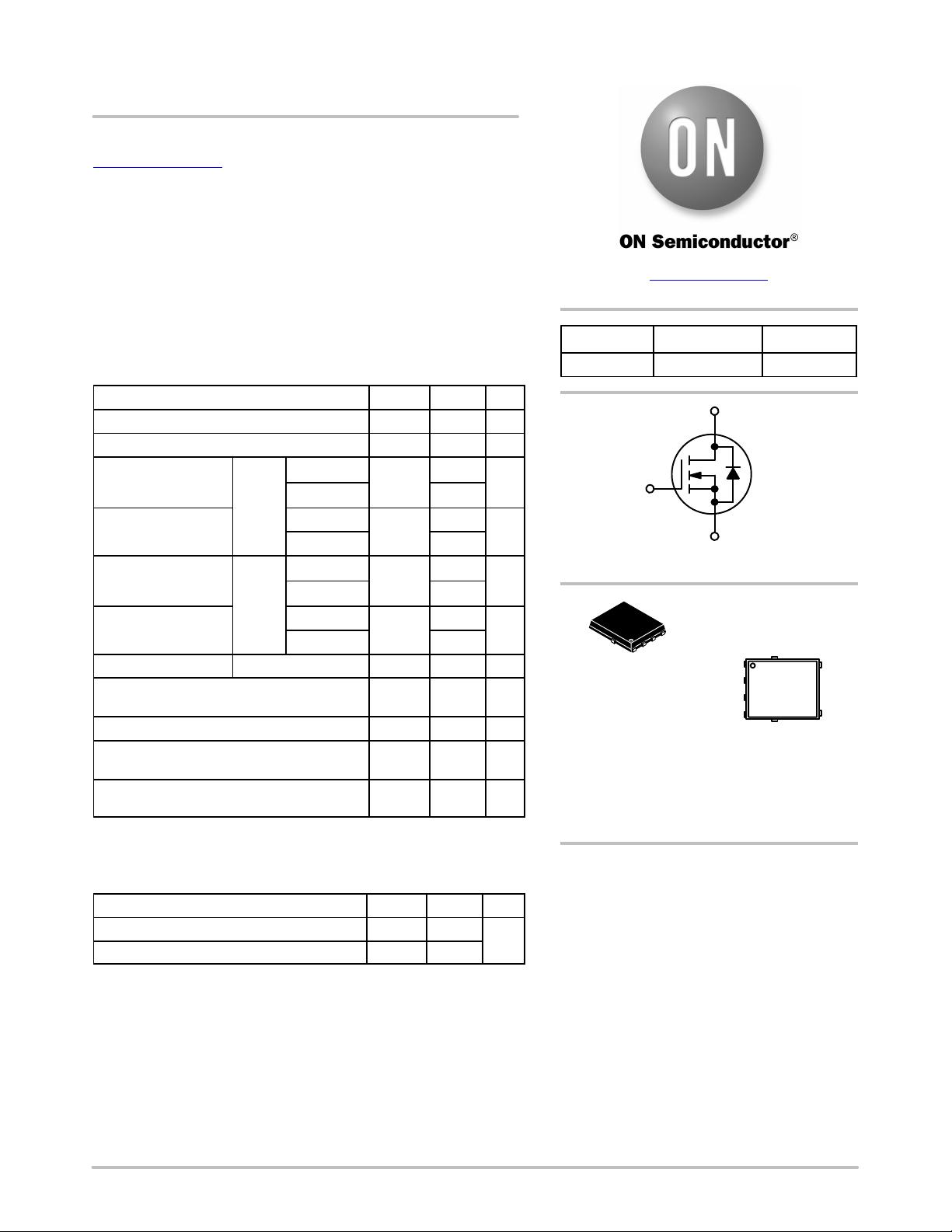
MOSFET - Power, Single
N-Channel
60 V, 3.0 mW, 150 A
Features
• Small Footprint (5x6 mm) for Compact Design
• Low R
DS(on)
to Minimize Conduction Losses
• Low Q
G
and Capacitance to Minimize Driver Losses
• These Devices are Pb−Free and are RoHS Compliant
MAXIMUM RATINGS (T
J
= 25°C unless otherwise noted)
Parameter
Symbol Value Unit
Drain−to−Source Voltage V
DSS
60 V
Gate−to−Source Voltage V
GS
±20 V
Continuous Drain
Current R
q
JC
(Notes 1, 3)
Steady
State
T
C
= 25°C
I
D
150
A
T
C
= 100°C 110
Power Dissipation
R
q
JC
(Note 1)
T
C
= 25°C
P
D
110
W
T
C
= 100°C 56
Continuous Drain
Current R
q
JA
(Notes 1, 2, 3)
Steady
State
T
A
= 25°C
I
D
28
A
T
A
= 100°C 20
Power Dissipation
R
q
JA
(Notes 1, 2)
T
A
= 25°C
P
D
3.7
W
T
A
= 100°C 1.9
Pulsed Drain Current
T
A
= 25°C, t
p
= 10 ms
I
DM
900 A
Operating Junction and Storage Temperature
Range
T
J
, T
stg
−55 to
+175
°C
Source Current (Body Diode) I
S
120 A
Single Pulse Drain−to−Source Avalanche
Energy (I
L(pk)
= 9 A)
E
AS
565 mJ
Lead Temperature for Soldering Purposes
(1/8″ from case for 10 s)
T
L
260 °C
Stresses exceeding those listed in the Maximum Ratings table may damage the
device. If any of these limits are exceeded, device functionality should not be
assumed, damage may occur and reliability may be affected.
THERMAL RESISTANCE MAXIMUM RATINGS
Parameter Symbol Value Unit
Junction−to−Case − Steady State
R
q
JC
1.3
°C/W
Junction−to−Ambient − Steady State (Note 2)
R
q
JA
40
1. The entire application environment impacts the thermal resistance values shown,
they are not constants and are only valid for the particular conditions noted.
2. Surface−mounted on FR4 board using a 650 mm
2
, 2 oz. Cu pad.
3. Maximum current for pulses as long as 1 second is higher but is dependent
on pulse duration and duty cycle.
MARKING
DIAGRAM
www.onsemi.com
5C628N = Specific Device Code
A = Assembly Location
Y = Year
W = Work Week
ZZ = Lot Traceability
5C628N
AYWZZ
V
(BR)DSS
R
DS(ON)
MAX I
D
MAX
60 V
3.0 mW @ 10 V
150 A
G (4)
S (1,2,3)
N−CHANNEL MOSFET
D (5)
S
S
S
G
D
D
D
D
DFN5
(SO−8FL)
CASE 488AA
STYLE 1
1
See detailed ordering, marking and shipping information in the
package dimensions section on page 5 of this data sheet.
ORDERING INFORMATION


 我的内容管理
展开
 我的资源
快来上传第一个资源
 我的收益 登录查看自己的收益
 我的积分
登录查看自己的积分
 我的C币
登录后查看C币余额
 我的收藏
我的收藏  我的下载
我的下载  下载帮助
下载帮助 
 前往需求广场,查看用户热搜

 信息提交成功