TI-BQ24780s
需积分: 5 94 浏览量
2023-04-10
11:31:09
上传
评论
收藏 1.22MB PDF 举报

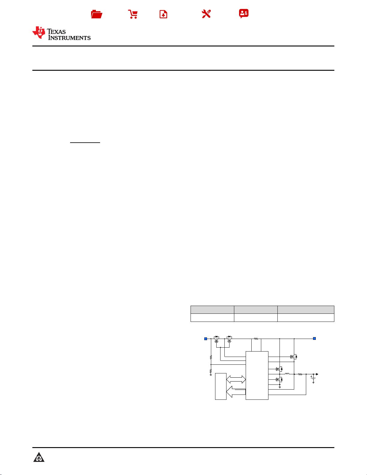
R
SR
Adapter
4.5-24V
HOST
bq24780S
Hybrid Power
Boost Charge
Controller
SYS
Battery
Pack
N-FET Driver
N-FET Driver
1S-4S
SMBus
IADP, ,PROCHOT
PMON, IDCHG
SMBus Controls V & I
with high accuracy
Adapter Detection
Enhanced Safety:
OCP, OVP, FET Short
Integration:
Loop Compensation; Soft-Start
Comparator, BTST Diode
R
AC
Product
Folder
Order
Now
Technical
Documents
Tools &
Software
Support &
Community
An IMPORTANT NOTICE at the end of this data sheet addresses availability, warranty, changes, use in safety-critical applications,
intellectual property matters and other important disclaimers. PRODUCTION DATA.
English Data Sheet: SLUSC27
bq24780S
ZHCSG48C –APRIL 2015–REVISED MARCH 2017
bq24780S 1 到到 4 节节混混合合动动力力升升压压模模式式电电池池充充电电控控制制器器
((支支持持电电源源监监视视和和处处理理器器热热量量监监视视))
1
1 特特性性
1
• 支持混合动力升压模式的工业创新型充电控制器
– 适配器和电池一同为系统供电,支持 Intel
®
CPU
Turbo 模式
– 进入升压模式的超快瞬态响应时间为 150µs
– 混合动力升压模式由 4.5 至 24V 系统供电
– 1 到 4 节电池由 4.5 至 24V 适配器充电
• 高精度电源和电流监视,实现 CPU 节能
– 全面的 PROCHOT 功能
– ± 2% 电流监视精度
– ± 5% 系统电源监视精度 (PMON)
• 可自动选择适配器或电池作为 NMOS 电源
– ACFET 在 100µs 内快速接通
• 可编程的输入电流、充电电压、充电和放电电流限
值
– ±0.4% 充电电压(16mV 步长)
– ±2% 输入电流(128mA/步长)
– ±2% 充电电流(64mA/步长)
– ±2% 放电电流(512mA/步长)
• 高集成
– 电池 LEARN(学习)功能
– 电池状态监视器
– 升压模式指示器
– 环路补偿
– BTST 二极管
• 针对 过压保护、 过流保护、电池、电感器和
MOSFET 短路保护的增强型安全特性
• 开关频率:600kHz、800kHz 和
1MHz
• 可对 ILIM 引脚进行实时系统控制以限制充电电流
和放电电流
• 适用于 Energy Star 的 0.65mA 适配器待机静态电
流
2 应应用用
• 笔记本、超极本、可拆卸平板电脑和常规平板电脑
• 手持式终端
• 工业用和医疗用设备
• 便携式设备
3 说说明明
bq24780S 器件是一款高效同步电池充电器,所含元件
数较少,适用于空间受限的多化合物电池充电 应用。
bq24780S 器件支持混合动力升压模式(之前称之为
“涡轮升压模式”)。当系统电源需求突然超过适配器最
大电源水平时,可利用此模式对系统放电。这样适配器
就不会受损。
bq24780S 器件利用两个电荷泵分别驱动 N 通道
MOSFET(ACFET、RBFET 和 BATFET),以便自
动选择系统电源。
系统电源管理微控制器可以通过 SMBus 对具有较高调
节精度的输入电流、充电电流、放电电流和充电电压
DAC 进行编程。
bq24780S 器件可监视适配器电流 (IADP)、电池放电
电流 (IDCHG) 和系统电源 (PMON),以便主机根据需
要控制 CPU 速度回落或减少系统电源。
bq24780S 器件可对 1、2、3 或 4 节串联锂离子电池
充电。
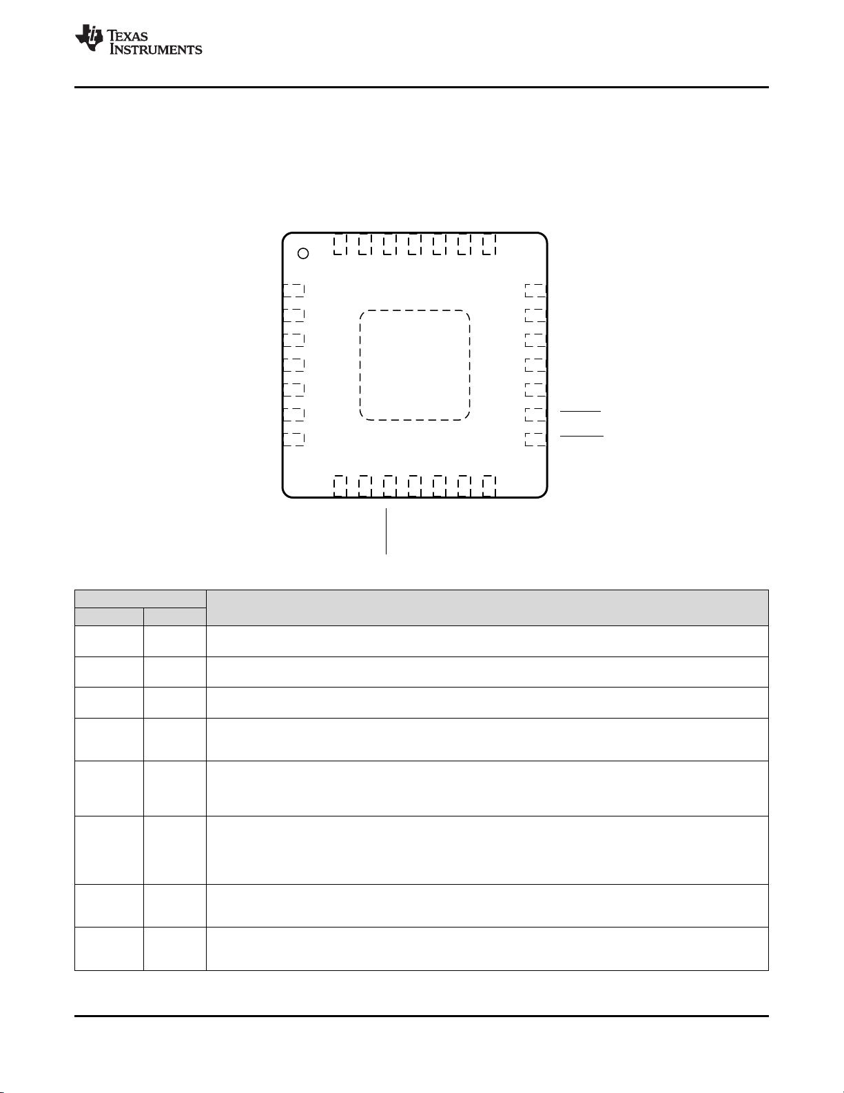
器器件件信信息息
(1)
器器件件型型号号 封封装装 封封装装尺尺寸寸((标标称称值值))
bq24780S WQFN (28) 4.00 × 4.00mm
2
(1) 要了解所有可用封装,请见数据表末尾的可订购产品附录。


剩余55页未读,继续阅读
资源评论


duni0810
- 粉丝: 10
- 资源: 48


最新资源
- 蓝桥杯,作为全国软件和信息技术专业人才大赛的知名品牌,旨在促进软件和信息技术领域专业人才培养、推动产学研用有机结合、提高大学生的
- 智能车,作为现代汽车科技的重要发展方向,集合了环境感知、规划决策、多等级辅助驾驶等多种功能于一体,是计算机、现代传感、信息融合、
- 基于SylixOS人脸识别考勤系统用到Qt+OpenCV+ncnn源码+设计文档+算法文档.zip
- 模拟试题三.zip
- Ditto-粘贴板工具
- 毕设基于人脸识别的实验室智能考勤系统设计与开发MFC源码含模型onnx文件.zip
- 数字字母组合字典常用top7000
- 使用Python-OpenCV对多张图片进行全景图像拼接消除鬼影消除裂缝源码.zip
- 百度贴吧12.57.5.0.apk
- JavaScript,简称JS,是一种在Web开发中举足轻重的客户端脚本语言 它最初由Netscape公司的布兰登·艾奇在199
资源上传下载、课程学习等过程中有任何疑问或建议,欢迎提出宝贵意见哦~我们会及时处理!
点击此处反馈


