没有合适的资源?快使用搜索试试~ 我知道了~
PCA9535 datasheet
需积分: 1 0 下载量 139 浏览量
2024-02-19
10:22:53
上传
评论
收藏 184KB PDF 举报
温馨提示
试读
31页
The PCA9535 and PCA9535C are 24-pin CMoS devices that provide 16 bits of GeneralPurpose parallel inputOutput (GPlO) expansion for 12C-bus/SMBus applications and wasdeveloped to enhance the NXP Semiconductors family of 12C-bus l/0 expanders. Theimprovements include higher drive capability, 5 V l/0 tolerance, lower supply current.individual 1/0 configuration, and smaller packaging. l/0 expanders provide a simplesolution when additional l/0 is needed for ACPl power switches, sensors, push buttons.L
资源推荐
资源详情
资源评论
1. General description
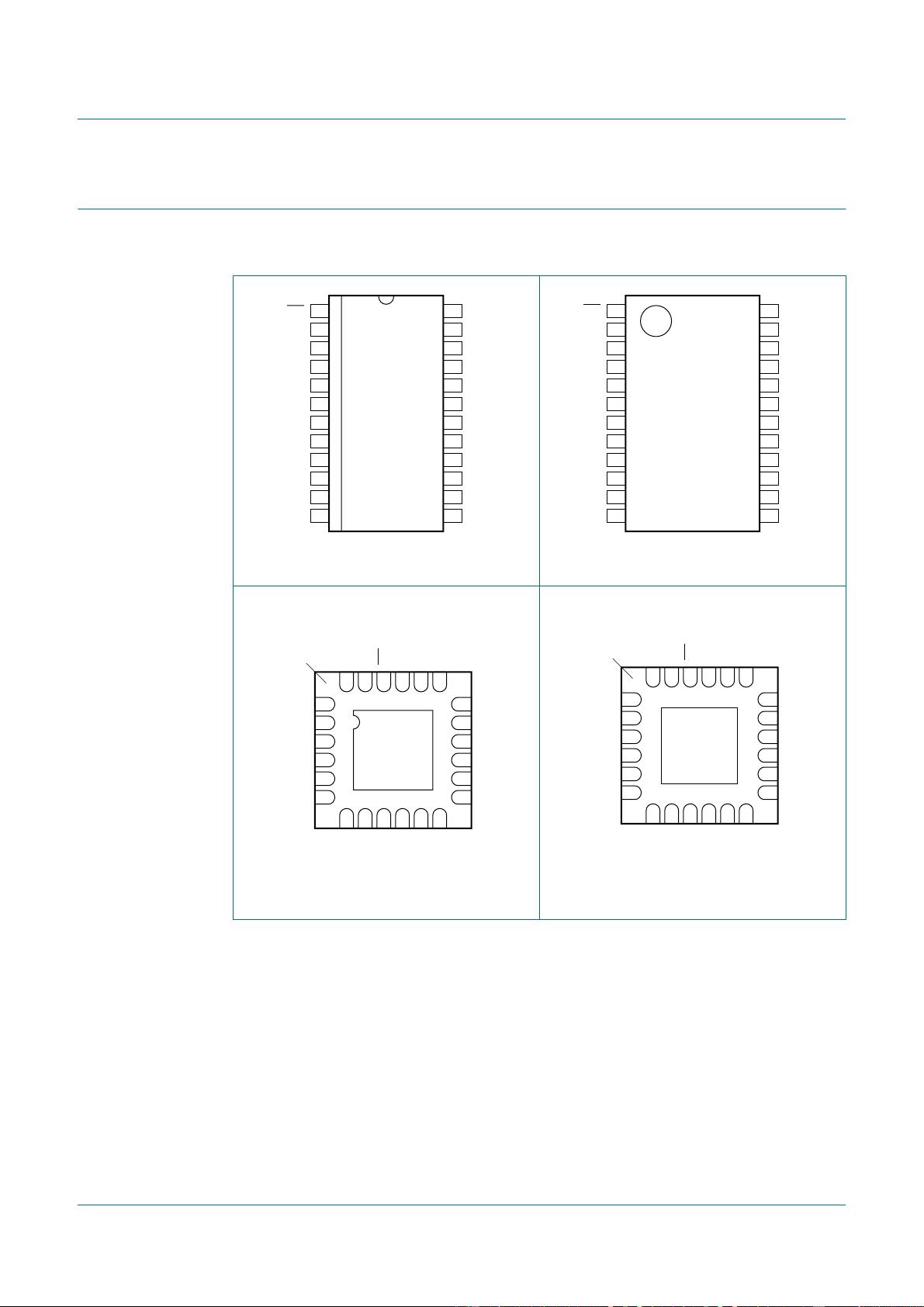
The PCA9535 and PCA9535C are 24-pin CMOS devices that provide 16 bits of General
Purpose parallel Input/Output (GPIO) expansion for I
2
C-bus/SMBus applications and was
developed to enhance the NXP Semiconductors family of I
2
C-bus I/O expanders. The
improvements include higher drive capability, 5 V I/O tolerance, lower supply current,
individual I/O configuration, and smaller packaging. I/O expanders provide a simple
solution when additional I/O is needed for ACPI power switches, sensors, push buttons,
LEDs, fans, etc.
The PCA9535 and PCA9535C consist of two 8-bit Configuration (Input or Output
selection), Input, Output and Polarity Inversion (active HIGH or active LOW operation)
registers. The system master can enable the I/Os as either inputs or outputs by writing to
the I/O configuration bits. The data for each input or output is kept in the corresponding
Input or Output register. The polarity of the read register can be inverted with the Polarity
Inversion register. All registers can be read by the system master. Although pin-to-pin and
I
2
C-bus address compatible with the PCF8575, software changes are required due to the
enhancements and are discussed in
Application Note AN469
.
The PCA9535 is identical to the PCA9555 except for the removal of the internal I/O pull-up
resistor which greatly reduces power consumption when the I/Os are held LOW.
The PCA9535C is identical to the PCA9535 except that all the I/O pins are
high-impedance open-drain outputs.
The PCA9535 and PCA9535C open-drain interrupt output is activated when any input
state differs from its corresponding Input Port register state and is used to indicate to the
system master that an input state has changed. The power-on reset sets the registers to
their default values and initializes the device state machine.
Three hardware pins (A0, A1, A2) vary the fixed I
2
C-bus address and allow up to eight
devices to share the same I
2
C-bus/SMBus. The fixed I
2
C-bus address of the PCA9535
and PCA9535C are the same as the PCA9555 allowing up to eight of these devices in any
combination to share the same I
2
C-bus/SMBus.
2. Features
n Operating power supply voltage range of 2.3 V to 5.5 V
n 5 V tolerant I/Os
n Polarity Inversion register
n Active LOW interrupt output
n Low standby current
n Noise filter on SCL/SDA inputs
PCA9535; PCA9535C
16-bit I
2
C-bus and SMBus, low power I/O port with interrupt
Rev. 05 — 15 September 2008 Product data sheet
PCA9535_PCA9535C_5 © NXP B.V. 2008. All rights reserved.
Product data sheet Rev. 05 — 15 September 2008 2 of 31
NXP Semiconductors
PCA9535; PCA9535C
16-bit I
2
C-bus and SMBus, low power I/O port with interrupt
n No glitch on power-up
n Internal power-on reset
n 16 I/O pins which default to 16 inputs
n 0 Hz to 400 kHz clock frequency
n ESD protection exceeds 2000 V HBM per JESD22-A114, 200 V MM per
JESD22-A115, and 1000 V CDM per JESD22-C101
n Latch-up testing is done to JEDEC Standard JESD78 which exceeds 100 mA
n Offered in four different packages: SO24, TSSOP24, HVQFN24 and HWQFN24
3. Ordering information
3.1 Ordering options
Table 1. Ordering information
Type number Package
Name Description Version
PCA9535D SO24 plastic small outline package; 24 leads;
body width 7.5 mm
SOT137-1
PCA9535PW TSSOP24 plastic thin shrink small outline package; 24 leads; body
width 4.4 mm
SOT355-1
PCA9535BS HVQFN24 plastic thermal enhanced very thin quad flat package;
no leads; 24 terminals; body 4 × 4 × 0.85 mm
SOT616-1
PCA9535HF HWQFN24 plastic thermal enhanced very very thin quad flat
package; no leads; 24 terminals; body 4 × 4 × 0.75 mm
SOT994-1
PCA9535CD SO24 plastic small outline package; 24 leads;
body width 7.5 mm
SOT137-1
PCA9535CPW TSSOP24 plastic thin shrink small outline package; 24 leads; body
width 4.4 mm
SOT355-1
PCA9535CHF HWQFN24 plastic thermal enhanced very very thin quad flat
package; no leads; 24 terminals; body 4 × 4 × 0.75 mm
SOT994-1
Table 2. Ordering options
Type number Topside mark Temperature range
PCA9535D PCA9535D T
amb
= −40 °C to +85 °C
PCA9535PW PCA9535PW T
amb
= −40 °C to +85 °C
PCA9535BS 9535 T
amb
= −40 °C to +85 °C
PCA9535HF P35H T
amb
= −40 °C to +85 °C
PCA9535CD PCA9535CD T
amb
= −40 °C to +85 °C
PCA9535CPW PCA9535C T
amb
= −40 °C to +85 °C
PCA9535CHF P35C T
amb
= −40 °C to +85 °C
PCA9535_PCA9535C_5 © NXP B.V. 2008. All rights reserved.
Product data sheet Rev. 05 — 15 September 2008 3 of 31
NXP Semiconductors
PCA9535; PCA9535C
16-bit I
2
C-bus and SMBus, low power I/O port with interrupt
4. Block diagram
Remark: All I/Os are set to inputs at reset.
Fig 1. Block diagram of PCA9535; PCA9535C
PCA9535
PCA9535C
POWER-ON
RESET
002aac217
I
2
C-BUS/SMBus
CONTROL
INPUT
FILTER
SCL
SDA
V
DD
INPUT/
OUTPUT
PORTS
IO0_0
V
SS
8-bit
write pulse
read pulse
IO0_2
IO0_1
IO0_3
IO0_4
IO0_5
IO0_6
IO0_7
INPUT/
OUTPUT
PORTS
IO1_0
8-bit
write pulse
read pulse
IO1_2
IO1_1
IO1_3
IO1_4
IO1_5
IO1_6
IO1_7
INT
A1
A0
A2
V
DD
PCA9535_PCA9535C_5 © NXP B.V. 2008. All rights reserved.
Product data sheet Rev. 05 — 15 September 2008 4 of 31
NXP Semiconductors
PCA9535; PCA9535C
16-bit I
2
C-bus and SMBus, low power I/O port with interrupt
5. Pinning information
5.1 Pinning
Fig 2. Pin configuration for SO24 Fig 3. Pin configuration for TSSOP24
Fig 4. Pin configuration for HVQFN24 Fig 5. Pin configuration for HWQFN24
PCA9535D
PCA9535CD
INT V
DD
A1 SDA
A2 SCL
IO0_0 A0
IO0_1 IO1_7
IO0_2 IO1_6
IO0_3 IO1_5
IO0_4 IO1_4
IO0_5 IO1_3
IO0_6 IO1_2
IO0_7 IO1_1
V
SS
IO1_0
002aac214
1
2
3
4
5
6
7
8
9
10
11
12
14
13
16
15
18
17
20
19
22
21
24
23
V
DD
SDA
SCL
A0
IO1_7
IO1_6
IO1_5
IO1_4
IO1_3
IO1_2
IO1_1
IO1_0
INT
A1
A2
IO0_0
IO0_1
IO0_2
IO0_3
IO0_4
IO0_5
IO0_6
IO0_7
V
SS
PCA9535PW
PCA9535CPW
002aac215
1
2
3
4
5
6
7
8
9
10
11
12
14
13
16
15
18
17
20
19
22
21
24
23
002aac216
PCA9535BS
Transparent top view
IO1_3
IO0_4
IO0_5
IO1_4
IO0_3 IO1_5
IO0_2 IO1_6
IO0_1 IO1_7
IO0_0 A0
IO0_6
IO0_7
V
SS
IO1_0
IO1_1
IO1_2
A2
A1
V
DD
SDA
SCL
terminal 1
index area
6
13
5
14
4 15
3 16
2 17
1
18
7
8
9
10
11
12
24
23
22
21
20
19
INT
002aac880
Transparent top view
IO1_3
IO0_4
IO0_5
IO1_4
IO0_3 IO1_5
IO0_2 IO1_6
IO0_1 IO1_7
IO0_0 A0
IO0_6
IO0_7
V
SS
IO1_0
IO1_1
IO1_2
A2
A1
INT
V
DD
SDA
SCL
terminal 1
index area
6
13
5
14
4 15
3 16
2 17
1
18
7
8
9
10
11
12
24
23
22
21
20
19
PCA9535HF
PCA9535CHF
PCA9535_PCA9535C_5 © NXP B.V. 2008. All rights reserved.
Product data sheet Rev. 05 — 15 September 2008 5 of 31
NXP Semiconductors
PCA9535; PCA9535C
16-bit I
2
C-bus and SMBus, low power I/O port with interrupt
5.2 Pin description
[1] HVQFN24 and HWQFN24 package die supply ground is connected to both the V
SS
pin and the exposed
center pad. The V
SS
pin must be connected to supply ground for proper device operation. For enhanced
thermal, electrical, and board-level performance, the exposed pad needs to be soldered to the board using
a corresponding thermal pad on the board, and for proper heat conduction through the board thermal vias
need to be incorporated in the PCB in the thermal pad region.
[2] PCA9535 I/Os are totem pole, whereas the I/Os on PCA9535C are open-drain.
Table 3. Pin description
Symbol Pin Description
SO24, TSSOP24 HVQFN24,
HWQFN24
INT 1 22 interrupt output (open-drain)
A1 2 23 address input 1
A2 3 24 address input 2
IO0_0 4 1 port 0 input/output
[2]
IO0_1 5 2
IO0_2 6 3
IO0_3 7 4
IO0_4 8 5
IO0_5 9 6
IO0_6 10 7
IO0_7 11 8
V
SS
12 9
[1]
supply ground
IO1_0 13 10 port 1 input/output
[2]
IO1_1 14 11
IO1_2 15 12
IO1_3 16 13
IO1_4 17 14
IO1_5 18 15
IO1_6 19 16
IO1_7 20 17
A0 21 18 address input 0
SCL 22 19 serial clock line
SDA 23 20 serial data line
V
DD
24 21 supply voltage
剩余30页未读,继续阅读
资源评论
denty
- 粉丝: 1
- 资源: 3
上传资源 快速赚钱
- 我的内容管理 展开
- 我的资源 快来上传第一个资源
- 我的收益 登录查看自己的收益
- 我的积分 登录查看自己的积分
- 我的C币 登录后查看C币余额
- 我的收藏
- 我的下载
- 下载帮助
安全验证
文档复制为VIP权益,开通VIP直接复制
信息提交成功