
TN-41-01: Calculating Memory System Power for DDR3
Introduction
PDF: 09005aef829559ff/Source: 09005aef828dcdbf Micron Technology, Inc., reserves the right to change products or specifications without notice.
TN41_01DDR3 Power.fm - Rev. B 8/07 EN
1 ©2007 Micron Technology, Inc. All rights reserved.
Products and specifications discussed herein are for evaluation and reference purposes only and are subject to change by
Micron without notice. Products are only warranted by Micron to meet Micron’s production data sheet specifications. All
information discussed herein is provided on an “as is” basis, without warranties of any kind.
Technical Note
Calculating Memory System Power for DDR3
Introduction
DDR3 SDRAM provides additional bandwidth over previous DDR and DDR2 SDRAM. In
addition to the premium performance, DDR3 has a lower operating voltage range. The
result can be a higher bandwidth performing system while consuming equal or less
system power. However, it is not always easy to determine the power consumption
within a system application from the data sheet specification.
This technical note details how DDR3 SDRAM consumes power and provides the tools
that system designers can use to estimate power consumption in any specific system. In
addition to offering tools and techniques for calculating system power, Micron’s DDR3-
1067 “Data Sheet Specifications” on page 20 and a DDR3 Power Spreadsheet Usage
Example on page 20 are provided.
Table 1 describes the command abbreviations found in the following sections.
DRAM Operation
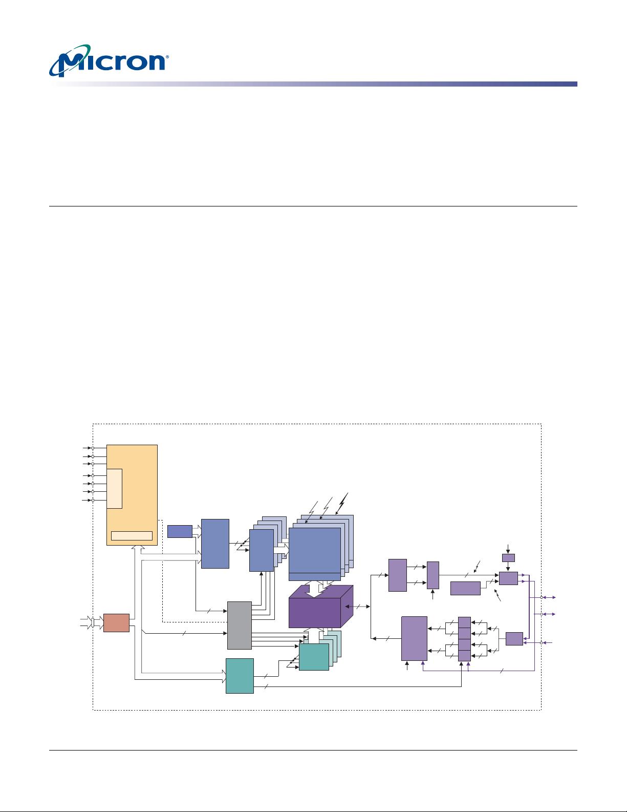
To estimate the power consumption of a DDR3 SDRAM, it is necessary to understand the
basic functionality of the device (see Figure 1 on page 2). The operation of a DDR3
device is similar to that of a DDR2. For both devices, the master operation of the DRAM
is controlled by clock enable (CKE).
If CKE is LOW, the input buffers are turned off. To allow the DRAM to receive commands,
CKE must be HIGH, thus enabling the input buffers and propagates the command/
address into the logic/decoders on the DRAM.
During normal operation, the first command sent to the DRAM is typically an ACT
command. This command selects a bank and row address. The data, which is stored in
the cells of the selected row, is then transferred from the array into the sense amplifiers.
The portion of the DRAM consuming power in the ACT command is shown in blue and
gold in Figure 1 on page 2.
Table 1: Abbreviation Definitions
Abbreviation Definition
ACT ACTIVATE
BL Burst length
BC Burst chop
PRE PRECHARGE
ODT On-die termination
RD READ
REF REFRESH
WR WRITE