没有合适的资源?快使用搜索试试~ 我知道了~
朝图LDO系列,朝图MOS系列,朝图DCDC系列
资源推荐
资源详情
资源评论
![rar](https://img-home.csdnimg.cn/images/20210720083606.png)
![exe](https://img-home.csdnimg.cn/images/20210720083343.png)
![zip](https://img-home.csdnimg.cn/images/20210720083736.png)
![pdf](https://img-home.csdnimg.cn/images/20210720083512.png)
![zip](https://img-home.csdnimg.cn/images/20210720083736.png)
![](https://csdnimg.cn/release/download_crawler_static/88745621/bg1.jpg)
5.5V 3A 1.2MHz Synchronous Step-Down Regulato
ZT3432
r
Features
• 2.7V to 5.5V Input Voltage Range
• 3A Continuous Output Current
• 1.2MHz Switching Frequency
• Built-in Short Protection
• Built-in Over Current Limit
• Built-in Over Voltage Protection
• PFM Mode for High Efficiency in Light Load
• High Efficiency: Up to 96%
• Internal Soft-Start
• Output Adjustable from 0.6V
• Over Temperature Protected
• Low Quiescent Current: 40μA
• Available in DFN3*3- 10 package
• -40°C to +85°C Temperature Range
Applications
• Cellular and Smart Phones
• Wireless and DSL Modems
• PDAs
General Description
• Portable Instruments
• Digital Still and Video Cameras
• PC Cards
The ZT3432 is a high-efficiency monolithic synchronous buck regulator using a constant frequency, current mode
architecture. The device is available in an adjustable version. The 2.7V to 5.5V input voltage range makes the
ZT3432 ideally suited for single Li-Ion battery powered applications. 100% duty cycle provides low dropout
operation, extending battery life in portable systems. PWM/PFM mode operation provides very low output ripple
voltage for noise sensitive applications. Switching frequency is internally set at 1.2MHz, allowing the use of small
surface mount inductors and capacitors. Low output voltages are easily supported with the 0.6V feedback reference
voltage.
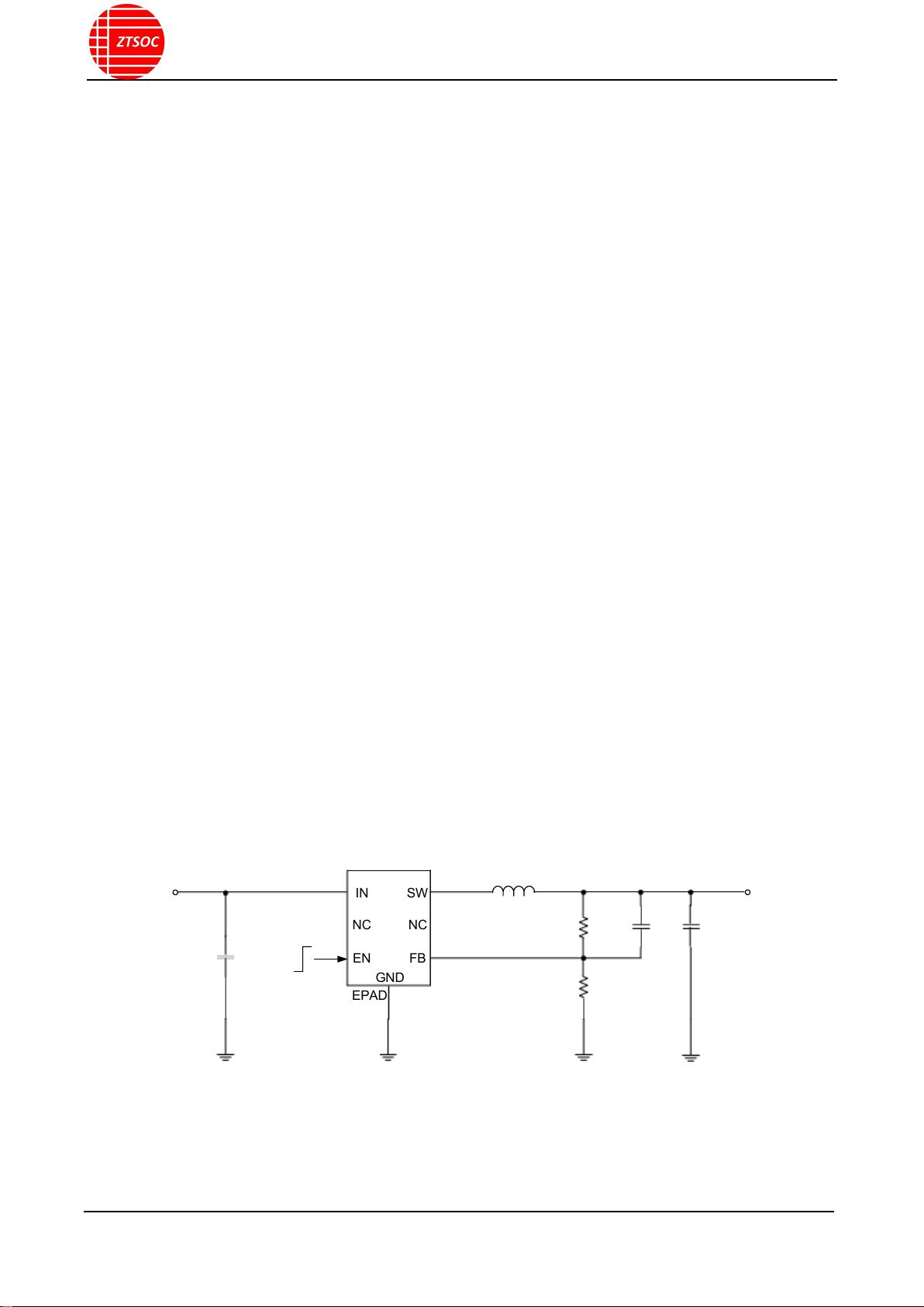
The ZT3432 requires a minimal number of readily available, external components and is available in a space saving
DFN3*3- 10 package.
Typical Application Circuit
V
OUT
IN SW
NC NC
EN FB
GND
EPAD
Basic Application Circuit
ON/
OFF
C
OUT
C
f f
C
IN
V
IN
R
2
R
1
L
1
江苏朝图微电子有限公司
http://ztsoc.com/
江苏朝图微电子有限公司
1
![](https://csdnimg.cn/release/download_crawler_static/88745621/bg2.jpg)
ZT3432
Pin Description
Pin Configuration
TOP VIEW
11
GND
(Exposed Pad)
1 10
2 9
8
4 7
5 6
DFN3×3-10
Top Marking: AMYLL (device code: AM, Y=year code, LL= lot number code)
Pin Description
Pin
Name Function
1/2 SW
Power Switch Output. It is the switch node connection to Inductor. This pin connects
to the drains of the internal P-ch and N-ch MOSFET switches.
3/4/7 NC
Not Connect.
5 EN
Chip Enable Pin. Drive EN above 1.2V to turn on the part. Drive EN below 0.6V to
turn it off. Do not leave EN floating.
6 FB
Output Voltage Feedback Pin. An internal resistive divider divides the output voltage
down for comparison to the internal reference voltage.
8/9/10 VIN
Power Supply Input. Must be closely decoupled to GND with a 10 µF or greater
ceramic capacitor.
11
GND/EPAD Ground Pin.
Order Information
(1)
Marking
Part No.
Model Description Package T/R Qty.
AMYLL 70301010 ZT3432
ZT3432 Buck, 2.7-5.5V, 3A, 1.2MHz,
VFB 0.6V, DFN3*3- 10
DFN3*3- 10 3000PCS
Note (1): All ZTSOC parts are Pb-Free and adhere to the RoHS directive.
SW
SW
NC 3
NC
EN
PVIN
PVIN
SVIN
NC
FB
江苏朝图微电子有限公司
http://ztsoc.com/
江苏朝图微电子有限公司
2
![](https://csdnimg.cn/release/download_crawler_static/88745621/bg3.jpg)
ZT3432
Specifications
Absolute Maximum Ratings
(1) (2)
Item Min
Max
Unit
V
IN
voltage -0.3 6 V
EN voltage -0.3 6 V
SW voltage -0.3
V
IN
+0.5V
V
FB voltage -0.3 6 V
Power dissipation
(3)
Internally Limited
Operating junction temperature, T
J
-40 150 °C
Storage temperature, T
stg
-55 150 °C
Lead Temperature (Soldering, 10sec.) 260 °C
Note (1): Exceeding these ratings may damage the device.
Note (2): The device is not guaranteed to function outside of its operating conditions.
Note (3): The maximum allowable power dissipation is a function of the maximum junction temperature, T
J(MAX)
,
the junction-to-ambient thermal resistance, R
θJA
, and the ambient temperature, T
A
. The maximum allowable power
dissipation at any ambient temperature is calculated using: P
D (MAX)
= (T
J(MAX)
− T
A
)/R
θJA
. Exceeding the maximum
allowable power dissipation causes excessive die temperature, and the regulator goes into thermal shutdown.
Internal thermal shutdown circuitry protects the device from permanent damage. Thermal shutdown engages at
T
J
=160°C (typical) and disengages at T
J
= 130°C (typical).
ESD Ratings
Item
Description
Value Unit
V
( ESD- HBM)
Human Body Model (HBM)
ANSI/ESDA/JEDEC JS-001-2014
Classification, Class: 2
±2000
V
V
( ESD- CDM)
Charged Device Mode (CDM)
ANSI/ESDA/JEDEC JS-002-2014
Classification, Class: C0b
±200
V
I
LATCH- UP
JEDEC STANDARD NO.78E APRIL 2016
Temperature Classification,
Class: I
±150
mA
Recommended Operating Conditions
Item Min
Max
Unit
Operating junction temperature
(1)
-40 125 °C
Operating temperature range -40 85 °C
Input voltage V
IN
2.7 5.5 V
Output current 0 3
A
Note (1): All limits specified at room temperature (TA = 25°C) unless otherwise specified. All room temperature
limits are 100% production tested. All limits at temperature extremes are ensured through correlation using standard
Statistical Quality Control (SQC) methods. All limits are used to calculate Average Outgoing Quality Level (AOQL).
江苏朝图微电子有限公司
http://ztsoc.com/
江苏朝图微电子有限公司
3
剩余11页未读,继续阅读
资源评论
![avatar-default](https://csdnimg.cn/release/downloadcmsfe/public/img/lazyLogo2.1882d7f4.png)
![avatar](https://profile-avatar.csdnimg.cn/default.jpg!1)
Ztsoc
- 粉丝: 44
- 资源: 2
上传资源 快速赚钱
我的内容管理 展开
我的资源 快来上传第一个资源
我的收益
登录查看自己的收益我的积分 登录查看自己的积分
我的C币 登录后查看C币余额
我的收藏
我的下载
下载帮助
![voice](https://csdnimg.cn/release/downloadcmsfe/public/img/voice.245cc511.png)
![center-task](https://csdnimg.cn/release/downloadcmsfe/public/img/center-task.c2eda91a.png)
安全验证
文档复制为VIP权益,开通VIP直接复制
![dialog-icon](https://csdnimg.cn/release/downloadcmsfe/public/img/green-success.6a4acb44.png)