


2.0 V, 32/16 kB Flash, smaRTClock, 12-bit ADC
C8051F410/1/2/3
Rev. 1.0 2/07 Copyright © 2007 by Silicon Laboratories C8051F41x
Analog Peripherals
- 12-Bit ADC
• ±1 LSB INL; no missing codes
• Programmable throughput up to 200 ksps
• Up to 24 external inputs
• Data dependent windowed interrupt generator
• Built-in temperature sensor (±3 °C)
-
Two 12-Bit Current Mode DACs
- Two Comparators
• Programmable hysteresis and response time
• Configurable as wake-up or reset source
- POR/Brownout Detector
- Voltage Reference—1.5, 2.2 V (programmable)
On-Chip Debug
- On-chip debug circuitry facilitates full-speed, non-
intrusive in-system debug (No emulator required)
- Provides breakpoints, single stepping
- Inspect/modify memory and registers
- Complete development kit
Supply Voltage 2.0 to 5.25 V
- Built-in LDO regulator: 2.1 or 2.5 V
High Speed 8051 µC Core
- Pipelined instruction architecture; executes 70% of
instructions in 1 or 2
system clocks
- Up to 50 MIPS throughput with
50 MHz system clock
- Expanded interrupt handler
Memory
- 2304 bytes internal data RAM (256 + 2048)
- 32/16 kB Flash; In-system programmable in
512
byte sectors
- 64 bytes battery-backed RAM (smaRTClock)
Digital Peripherals
- 24 port I/O; push-pull or open-drain, up to 5.25 V
tolerance
- Hardware SMBus™ (I2C™ Compatible), SPI™, and
UART serial ports available concurrently
- Four general purpose 16-bit counter/timers
- Programmable 16-bit counter/timer array with six
capture/compare modules, WDT
- Hardware smaRTClock operates down to 1 V with
64 bytes battery-backed RAM and backup voltage
regulator
Clock Sources
- Internal oscillators: 24.5 MHz 2% accuracy supports
UART operation; clock multiplier up to 50
MHz
- External oscillator: Crystal, RC, C, or Clock
(1 or 2 pin modes)
- smaRTClock oscillator: 32 kHz Crystal or
self-resonant oscillator
- Can switch between clock sources on-the-fly
32-PIN LQFP or 28-PIN 5x5 QFN
Temperature Range: –40 to +85 °C
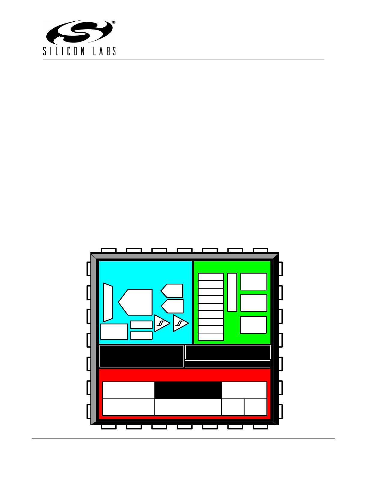
ANALOG
PERIPHERALS
12-bit
200 ksps
ADC
32/16 kB
ISP FLASH
2368 B
SRAM
POR
DEBUG
CIRCUITRY
FLEXIBLE
INTERRUPTS
8051 CPU
(50 MIPS)
TEMP
SENSOR
DIGITAL I/O
24.5 MHz PRECISION
INTERNAL OSCILLATOR
WITH CLOCK MULTIPLIER
HIGH-SPEED CONTROLLER CORE
A
M
U
X
CROSSBAR
VOLTAGE
COMPARATORS
+
-
WDT
UART
SMBus
PCA
Timer 0
Timer 1
Timer 2
Timer 3
Port 0
SPI
12-bit
IDAC
Port 1
12-bit
IDAC
Port 2
+
-
VREG
LOW FREQUENCY
INTERNAL OSCILLATOR
VREF
CRC
HARDWARE smaRTClock

C8051F410/1/2/3
2 Rev. 1.0
NOTES:

Rev. 1.0 3
C8051F410/1/2/3
Table of Contents
1. System Overview.................................................................................................... 19
1.1. CIP-51™ Microcontroller................................................................................... 25
1.1.1. Fully 8051 Compatible Instruction Set...................................................... 25
1.1.2. Improved Throughput............................................................................... 25
1.1.3. Additional Features .................................................................................. 25
1.2. On-Chip Debug Circuitry................................................................................... 26
1.3. On-Chip Memory............................................................................................... 27
1.4. Operating Modes .............................................................................................. 28
1.5. 12-Bit Analog to Digital Converter..................................................................... 29
1.6. Two 12-bit Current-Mode DACs........................................................................ 29
1.7. Programmable Comparators............................................................................. 30
1.8. Cyclic Redundancy Check Unit......................................................................... 31
1.9. Voltage Regulator ............................................................................................. 31
1.10.Serial Ports....................................................................................................... 31
1.11.smaRTClock (Real Time Clock) ....................................................................... 32
1.12.Port Input/Output .............................................................................................. 33
1.13.Programmable Counter Array........................................................................... 34
2. Absolute Maximum Ratings .................................................................................. 35
3. Global DC Electrical Characteristics .................................................................... 36
4. Pinout and Package Definitions............................................................................ 41
5. 12-Bit ADC (ADC0).................................................................................................. 51
5.1. Analog Multiplexer ............................................................................................ 51
5.2. Temperature Sensor......................................................................................... 52
5.3. ADC0 Operation................................................................................................ 52
5.3.1. Starting a Conversion............................................................................... 53
5.3.2. Tracking Modes........................................................................................ 53
5.3.3. Timing....................................................................................................... 54
5.3.4. Burst Mode............................................................................................... 56
5.3.5. Output Conversion Code.......................................................................... 57
5.3.6. Settling Time Requirements..................................................................... 58
5.4. Programmable Window Detector...................................................................... 63
5.4.1. Window Detector In Single-Ended Mode ................................................. 66
6. 12-Bit Current Mode DACs (IDA0 and IDA1) ........................................................ 69
6.1. IDAC Output Scheduling................................................................................... 69
6.1.1. Update Output On-Demand ..................................................................... 69
6.1.2. Update Output Based on Timer Overflow ................................................ 70
6.1.3. Update Output Based on CNVSTR Edge................................................. 70
6.2. IDAC Output Mapping....................................................................................... 70
6.3. IDAC External Pin Connections........................................................................ 73
7. Voltage Reference.................................................................................................. 77
8. Voltage Regulator (REG0)...................................................................................... 81
9. Comparators ......................................................................................................... 83

C8051F410/1/2/3
4 Rev. 1.0
10.CIP-51 Microcontroller ........................................................................................... 93
10.1.Instruction Set................................................................................................... 94
10.1.1.Instruction and CPU Timing ..................................................................... 94
10.1.2.MOVX Instruction and Program Memory ................................................. 95
10.2.Register Descriptions ....................................................................................... 98
10.3.Power Management Modes............................................................................ 101
10.3.1.Idle Mode ............................................................................................... 102
10.3.2.Stop Mode.............................................................................................. 102
10.3.3.Suspend Mode....................................................................................... 102
11.Memory Organization and SFRs......................................................................... 103
11.1.Program Memory............................................................................................ 103
11.2.Data Memory.................................................................................................. 104
11.3.General Purpose Registers ............................................................................ 104
11.4.Bit Addressable Locations.............................................................................. 104
11.5.Stack............................................................................................................... 104
11.6.Special Function Registers............................................................................. 105
12.Interrupt Handler .................................................................................................. 110
12.1.MCU Interrupt Sources and Vectors............................................................... 110
12.2.Interrupt Priorities ........................................................................................... 110
12.3.Interrupt Latency............................................................................................. 110
12.4.Interrupt Register Descriptions....................................................................... 112
12.5.External Interrupts .......................................................................................... 117
13.Prefetch Engine.................................................................................................... 119
14.Cyclic Redundancy Check Unit (CRC0) ............................................................. 121
14.1.CRC Algorithm................................................................................................ 121
14.2.Preparing for a CRC Calculation .................................................................... 123
14.3.Performing a CRC Calculation ....................................................................... 123
14.4.Accessing the CRC0 Result ........................................................................... 123
14.5.CRC0 Bit Reverse Feature............................................................................. 123
15.Reset Sources....................................................................................................... 127
15.1.Power-On Reset............................................................................................. 128
15.2.Power-Fail Reset / VDD Monitor .................................................................... 129
15.3.External Reset................................................................................................ 130
15.4.Missing Clock Detector Reset ........................................................................ 130
15.5.Comparator0 Reset ........................................................................................ 130
15.6.PCA Watchdog Timer Reset .......................................................................... 131
15.7.Flash Error Reset ........................................................................................... 131
15.8.smaRTClock (Real Time Clock) Reset........................................................... 132
15.9.Software Reset............................................................................................... 132
16.Flash Memory ....................................................................................................... 135
16.1.Programming The Flash Memory................................................................... 135
16.1.1.Flash Lock and Key Functions............................................................... 135
16.1.2.Flash Erase Procedure .......................................................................... 135
16.1.3.Flash Write Procedure ........................................................................... 136
16.2.Non-volatile Data Storage .............................................................................. 137

Rev. 1.0 5
C8051F410/1/2/3
16.3.Security Options ............................................................................................. 137
16.4.Flash Write and Erase Guidelines.................................................................. 139
16.4.1.VDD Maintenance and the VDD Monitor ............................................... 139
16.4.2.16.4.2 PSWE Maintenance.................................................................... 140
16.4.3.System Clock ......................................................................................... 140
16.5.Flash Read Timing ......................................................................................... 142
17.External RAM........................................................................................................ 145
18.Port Input/Output.................................................................................................. 147
18.1.Priority Crossbar Decoder .............................................................................. 149
18.2.Port I/O Initialization ....................................................................................... 151
18.3.General Purpose Port I/O............................................................................... 154
19.Oscillators............................................................................................................. 165
19.1.Programmable Internal Oscillator................................................................... 165
19.1.1.Internal Oscillator Suspend Mode.......................................................... 166
19.2.External Oscillator Drive Circuit...................................................................... 168
19.2.1.Clocking Timers Directly Through the External Oscillator...................... 168
19.2.2.External Crystal Example....................................................................... 168
19.2.3.External RC Example............................................................................. 170
19.2.4.External Capacitor Example................................................................... 170
19.3.Clock Multiplier ............................................................................................... 172
19.4.System Clock Selection.................................................................................. 174
20.smaRTClock (Real Time Clock)........................................................................... 177
20.1.smaRTClock Interface.................................................................................... 178
20.1.1.smaRTClock Lock and Key Functions ................................................... 178
20.1.2.Using RTC0ADR and RTC0DAT to Access
smaRTClock Internal Registers.............................................................. 178
20.1.3.smaRTClock Interface Autoread Feature............................................... 178
20.1.4.RTC0ADR Autoincrement Feature......................................................... 179
20.2.smaRTClock Clocking Sources...................................................................... 182
20.2.1.Using the smaRTClock Oscillator in Crystal Mode ................................ 182
20.2.2.Using the smaRTClock Oscillator in Self-Oscillate Mode ...................... 182
20.2.3.Automatic Gain Control (Crystal Mode Only)......................................... 183
20.2.4.smaRTClock Bias Doubling ................................................................... 183
20.2.5.smaRTClock Missing Clock Detector..................................................... 183
20.3.smaRTClock Timer and Alarm Function......................................................... 185
20.3.1.Setting and Reading the smaRTClock Timer Value............................... 185
20.3.2.Setting a smaRTClock Alarm................................................................. 186
20.4.Backup Regulator and RAM........................................................................... 187
21.SMBus ................................................................................................................... 191
21.1.Supporting Documents................................................................................... 192
21.2.SMBus Configuration...................................................................................... 192
21.3.SMBus Operation ........................................................................................... 192
21.3.1.Arbitration............................................................................................... 193
21.3.2.Clock Low Extension.............................................................................. 193
21.3.3.SCL Low Timeout................................................................................... 194


