没有合适的资源?快使用搜索试试~ 我知道了~
TI的MSP430FW429数据手册/规格书下载
需积分: 9 0 下载量 185 浏览量
2022-09-21
15:43:33
上传
评论
收藏 1.47MB PDF 举报
温馨提示
试读
62页
MSP430FW429下载链接:https://www.wengexin.com/general_MCU_info?modelid=9595563
资源推荐
资源详情
资源评论
MSP430FW429, MSP430FW428
MSP430FW427, MSP430FW425, MSP430FW423
www.ti.com
SLAS383E –OCTOBER 2003–REVISED DECEMBER 2013
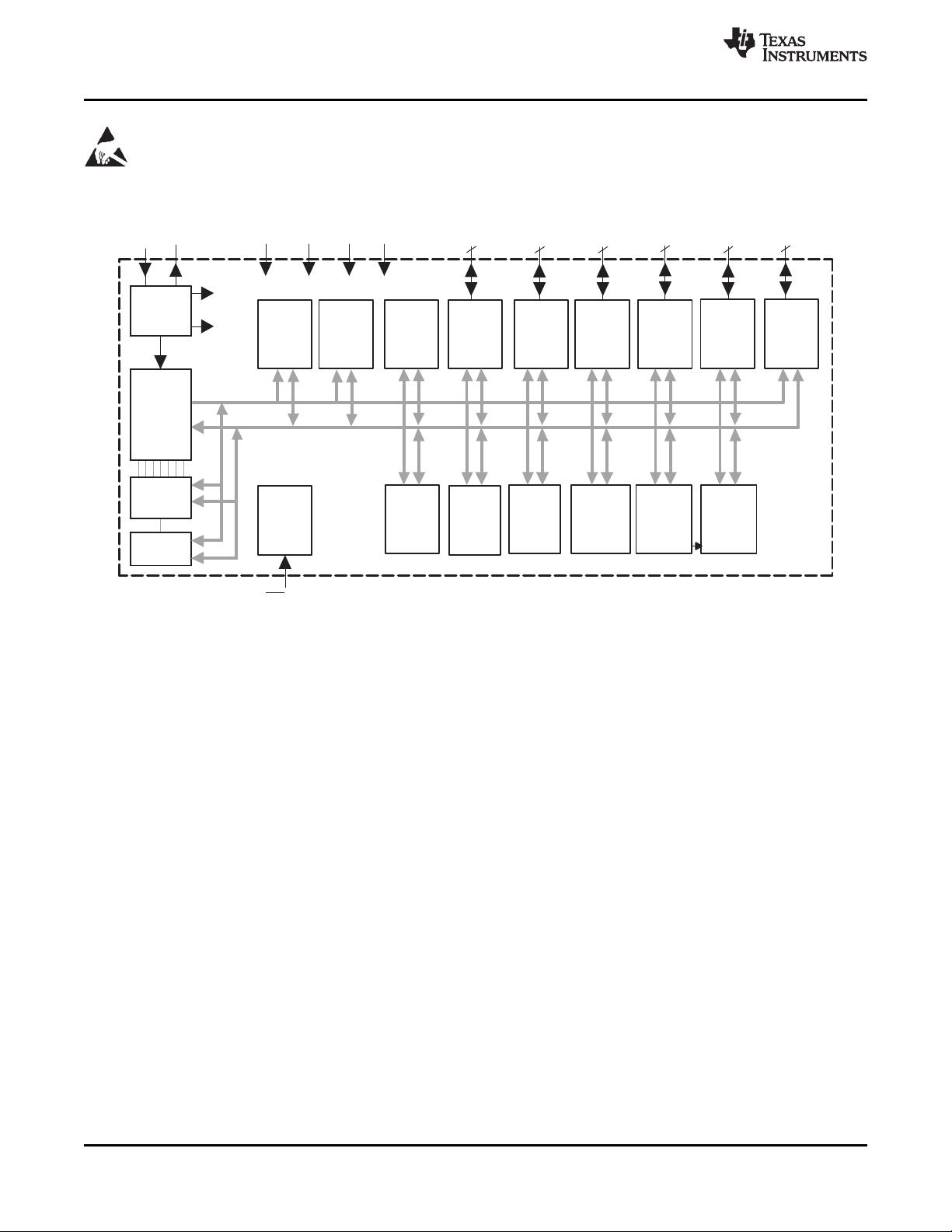
MSP430FW42x Mixed-Signal Microcontroller
1
FEATURES
2
• Low Supply Voltage Range: 1.8 V to 3.6 V
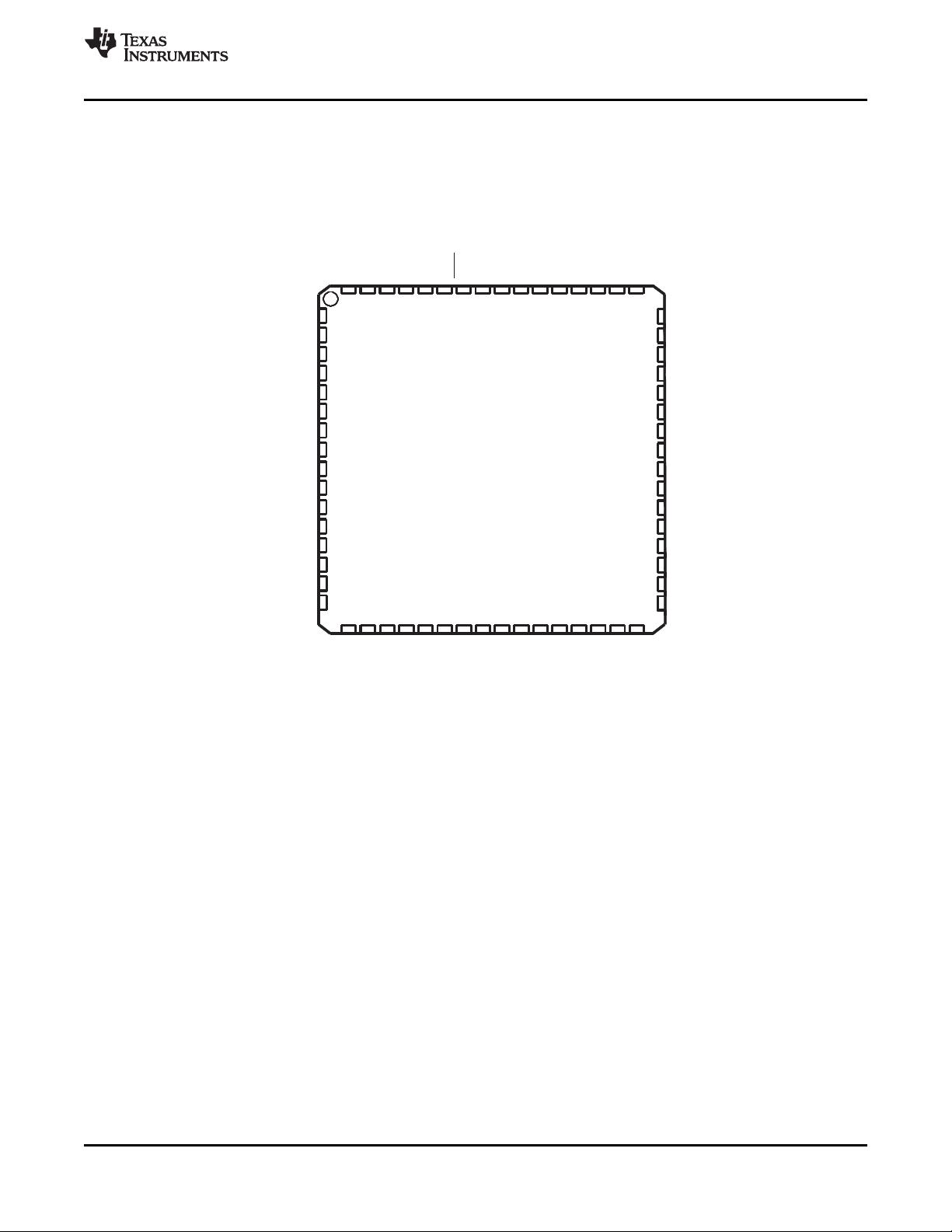
• Available in 64-Pin Quad Flat Pack (QFP)
• Ultra-Low-Power Consumption: • For Complete Module Descriptions, See the
MSP430x4xx Family User's Guide, Literature
– Active Mode: 200 µA at 1 MHz, 2.2 V
Number SLAU056
– Standby Mode: 0.7 µA
– Off Mode (RAM Retention): 0.1 µA
APPLICATIONS
• Five Power-Saving Modes
• Analog Sensor Systems
• Wake Up From Standby Mode in Less Than
• Digital Sensor Systems
6 µs
• Gas, Heat, or Water Meters
• Frequency-Locked Loop, FLL+
• Industrial Meters
• 16-Bit RISC Architecture,
• Hand-Held Meters
125-ns Instruction Cycle Time
• Scan Interface for Background Water, Heat,
DESCRIPTION
and Gas Volume Measurement
The Texas Instruments MSP430™ family of ultra-low-
• 16-Bit Timer_A With Three Capture/Compare
power microcontrollers consists of several devices
Registers
featuring different sets of peripherals targeted for
• 16-Bit Timer_A With Five Capture/Compare
various applications. The architecture, combined with
five low-power modes, is optimized to achieve
Registers
extended battery life in portable measurement
• Integrated LCD Driver for Up to 96 Segments
applications. The device features a powerful 16-bit
• On-Chip Comparator
RISC CPU, 16-bit registers, and constant generators
• Serial Onboard Programming, No External that contribute to maximum code efficiency. The
digitally controlled oscillator (DCO) allows the device
Programming Voltage Needed Programmable
to wake up from low-power modes to active mode in
Code Protection by Security Fuse
less than 6 µs.
• Brownout Detector
The MSP430FW42x series are microcontroller
• Supply Voltage Supervisor and Monitor With
configurations with two built-in 16-bit timers, a
Programmable Level Detection
comparator, 96 LCD segment drive capability, a scan
• Bootstrap Loader (BSL) in Flash Devices
interface, and 48 I/O pins.
• Family Members Include:
Typical applications include sensor systems that
– MSP430FW423
capture analog signals, convert them to digital values,
8KB + 256B Flash Memory, 256B RAM
and process the data and transmit them to a host
system. The comparator and timers make the
– MSP430FW425
configurations ideal for gas, heat, and water meters,
16KB + 256B Flash Memory, 512B RAM
industrial meters, counter applications, and hand-held
– MSP430FW427
meters.
32KB + 256B Flash Memory, 1KB RAM
– MSP430FW428
48KB + 256B Flash Memory, 2KB RAM
– MSP430FW429
60KB + 256B Flash Memory, 2KB RAM
1
Please be aware that an important notice concerning availability, standard warranty, and use in critical applications of
Texas Instruments semiconductor products and disclaimers thereto appears at the end of this data sheet.
2MSP430 is a trademark of Texas Instruments.
PRODUCTION DATA information is current as of publication date.
Copyright © 2003–2013, Texas Instruments Incorporated
Products conform to specifications per the terms of the Texas
Instruments standard warranty. Production processing does not
necessarily include testing of all parameters.
Comparator_
A
DV
CC
DV
SS
AV
CC
AV
SS
RST
/NMI
P2
Flash
60KB/48KB
32KB
16KB
8KB
RAM
2KB
1KB
512B
256B
Watchdog
Timer
WDT
15/16-Bit
Port 2
8 I/O
Interrupt
Capability
POR/
Multilevel
SVS/
Brownout
Basic
Timer 1
1 Interrupt
Vector
LCD
96
Segments
1,2,3,4 MUX
f
LCD
8
MCLK
XOUT
JTAG
Interface
XIN
SMCLK
ACLK
MDB
MAB
Emulation
P3
Port 3
8 I/O
8
Module
Timer1_A5
5 CC Reg
P1
Port 1
8 I/O
Interrupt
Capability
8
P4
Port 4
8 I/O
8
Scan IF
Oscillator
FLL+
8 MHz
CPU
incl. 16
Registers
P5
Port 5
8 I/O
8
P6
Port 6
8 I/O
8
Timer0_A3
3 CC Reg
MSP430FW429, MSP430FW428
MSP430FW427, MSP430FW425, MSP430FW423
SLAS383E –OCTOBER 2003–REVISED DECEMBER 2013
www.ti.com
This integrated circuit can be damaged by ESD. Texas Instruments recommends that all integrated circuits be handled with
appropriate precautions. Failure to observe proper handling and installation procedures can cause damage.
ESD damage can range from subtle performance degradation to complete device failure. Precision integrated circuits may be more
susceptible to damage because very small parametric changes could cause the device not to meet its published specifications.
Functional Block Diagram
2 Submit Documentation Feedback Copyright © 2003–2013, Texas Instruments Incorporated
Product Folder Links: MSP430FW429 MSP430FW428 MSP430FW427 MSP430FW425 MSP430FW423
17 18 19 20 21 22 23 24 25 26 27 28 29 30 31 32
64 63 62 61 60 59 58 57 56 55 54 53 52 51 50 49
P1.5/TA0CLK/ACLK
P6.2/SIFCH2
P6.1/SIFCH1
P6.0/SIFCH0
RST/NMI
TCK
TMS
TDI/TCLK
TDO/TDI
P1.0/TA0.0
P1.1/TA0.0/MCLK
P1.2/TA0.1
P1.3/TA1.0/SVSOUT
P1.4/TA1.0
P4.4/S5
P4.3/S6
P4.2/S7
P4.1/S8
P4.0/S9
P3.7/S10
P3.6/S11
P3.5/S12
P3.4/S13
P3.3/S14
P3.2/S15
P3.1/S16
P3.0/S17
P2.7/SIFCLKG/S18
P2.6/CAOUT/S19
P2.5/TA1CLK/S20
48
47
46
45
44
43
42
41
40
39
38
37
36
35
34
33
P1.6/CA0
P1.7/CA1
P2.0/TA0.2
P2.1/TA1.1
P5.7/R33
P5.6/R23
P5.5/R13
R03
P5.4/COM3
P5.3/COM2
P5.2/COM1
COM0
P2.2/TA1.2/S23
P2.4/TA1.4/S21
P2.3/TA1.3/S22
1
2
3
4
5
6
7
8
9
10
11
12
13
14
15
16
P6.3/SIFCH3/SIFCAOUT
P6.4/SIFCI0
P6.5/SIFCI1
P6.6/SIFCI2/SIFDACOUT
P6.7/SIFCI3/SVSIN
SIFCI
XIN
XOUT
SIFVSS
SIFCOM
P5.1/S0
P5.0/S1
P4.7/S2
P4.5/S4
P4.6/S3
MSP430xW42x
AV
CC
DV
SS
AV
SS
DV
CC
MSP430FW429, MSP430FW428
MSP430FW427, MSP430FW425, MSP430FW423
www.ti.com
SLAS383E –OCTOBER 2003–REVISED DECEMBER 2013
Pin Designation
Copyright © 2003–2013, Texas Instruments Incorporated Submit Documentation Feedback 3
Product Folder Links: MSP430FW429 MSP430FW428 MSP430FW427 MSP430FW425 MSP430FW423
MSP430FW429, MSP430FW428
MSP430FW427, MSP430FW425, MSP430FW423
SLAS383E –OCTOBER 2003–REVISED DECEMBER 2013
www.ti.com
Table 1. Terminal Functions
TERMINAL
I/O DESCRIPTION
NAME NO.
AV
CC
64 Analog supply voltage, positive terminal. Supplies SVS, brownout, oscillator, comparator_A,
scan IF AFE, port 6, and LCD resistive divider circuitry; must not power up prior to DV
CC
.
AV
SS
62 Analog supply voltage, negative terminal. Supplies SVS, brownout, oscillator, comparator_A,
scan IF AFE. and port 6. Must be externally connected to DV
SS
. Internally connected to DV
SS
.
DV
CC
1 Digital supply voltage, positive terminal.
DV
SS
63 Digital supply voltage, negative terminal.
SIFVSS 10 Scan IF AFE reference supply voltage.
P1.0/TA0.0 53 I/O General-purpose digital I/O
Timer0_A. Capture: CCI0A input, compare: Out0 output
BSL transmit
P1.1/TA0.0/MCLK 52 I/O General-purpose digital I/O
Timer0_A. Capture: CCI0B input
MCLK output
BSL receive
Note: TA0.0 is only an input on this pin.
P1.2/TA0.1 51 I/O General-purpose digital I/O
Timer0_A, capture: CCI1A input, compare: Out1 output
P1.3/TA1.0/SVSOUT 50 I/O General-purpose digital I/O
Timer1_A, capture: CCI0B input
SVS: output of SVS comparator
Note: TA1.0 is only an input on this pin.
P1.4/TA1.0 49 I/O General-purpose digital I/O
Timer1_A, capture: CCI0A input, compare: Out0 output
P1.5/TA0CLK/ACLK 48 I/O General-purpose digital I/O
Input of Timer0_A clock
Output of ACLK
P1.6/CA0 47 I/O General-purpose digital I/O
Comparator_A input
P1.7/CA1 46 I/O General-purpose digital I/O
Comparator_A input
P2.0/TA0.2 45 I/O General-purpose digital I/O
Timer0_A, capture: CCI2A input, compare: Out2 output
P2.1/TA1.1 44 I/O General-purpose digital I/O
Timer0_A, capture: CCI1A input, compare: Out1 output
P2.2/TA1.2/S23 35 I/O General-purpose digital I/O
Timer1_A, capture: CCI2A input, compare: Out2 output
LCD segment output 23
(1)
P2.3/TA1.3/S22 34 I/O General-purpose digital I/O
Timer1_A, capture: CCI3A input, compare: Out3 output
LCD segment output 22
(1)
P2.4/TA1.4/S21 33 I/O General-purpose digital I/O
Timer1_A, capture: CCI4A input, compare: Out4 output
LCD segment output 21
(1)
P2.5/TA1CLK/S20 32 I/O General-purpose digital I/O
Iinput of Timer1_A clock
LCD segment output 20
(1)
P2.6/CAOUT/S19 31 I/O General-purpose digital I/O
Comparator_A output
LCD segment output 19
(1)
P2.7/SIFCLKG/S18 30 I/O General-purpose digital I/O
Scan IF, signal SIFCLKG from internal clock generator
LCD segment output 18
(1)
P3.0/S17 29 I/O General-purpose digital I/O
LCD segment output 17
(1)
P3.1/S16 28 I/O General-purpose digital I/O
LCD segment output 16
(1)
(1) LCD function selected automatically when applicable LCD module control bits are set, not with PxSEL bits.
4 Submit Documentation Feedback Copyright © 2003–2013, Texas Instruments Incorporated
Product Folder Links: MSP430FW429 MSP430FW428 MSP430FW427 MSP430FW425 MSP430FW423
MSP430FW429, MSP430FW428
MSP430FW427, MSP430FW425, MSP430FW423
www.ti.com
SLAS383E –OCTOBER 2003–REVISED DECEMBER 2013
Table 1. Terminal Functions (continued)
TERMINAL
I/O DESCRIPTION
NAME NO.
P3.2/S15 27 I/O General-purpose digital I/O
LCD segment output 15
(1)
P3.3/S14 26 I/O General-purpose digital I/O
LCD segment output 14
(1)
P3.4/S13 25 I/O General-purpose digital I/O
LCD segment output 13
(1)
P3.5/S12 24 I/O General-purpose digital I/O
LCD segment output 12
(1)
P3.6/S11 23 I/O General-purpose digital I/O
LCD segment output 11
(1)
P3.7/S10 22 I/O General-purpose digital I/O
LCD segment output 10
(1)
P4.0/S9 21 I/O General-purpose digital I/O
LCD segment output 9
(1)
P4.1/S8 20 I/O General-purpose digital I/O
LCD segment output 8
(2)
P4.2/S7 19 I/O General-purpose digital I/O
LCD segment output 7
(2)
P4.3/S6 18 I/O General-purpose digital I/O
LCD segment output 6
(2)
P4.4/S5 17 I/O General-purpose digital I/O
LCD segment output 5
(2)
P4.5/S4 16 I/O General-purpose digital I/O
LCD segment output 4
(2)
P4.6/S3 15 I/O General-purpose digital I/O
LCD segment output 3
(2)
P4.7/S2 14 I/O General-purpose digital I/O
LCD segment output 2
(2)
P5.0/S1 13 I/O General-purpose digital I/O
LCD segment output 1
(2)
P5.1/S0 12 I/O General-purpose digital I/O
LCD segment output 0
(2)
COM0 36 O Common output. COM0-3 are used for LCD backplanes
P5.2/COM1 37 I/O General-purpose digital I/O
Common output. COM0-3 are used for LCD backplanes
P5.3/COM2 38 I/O General-purpose digital I/O
Common output. COM0-3 are used for LCD backplanes
P5.4/COM3 39 I/O General-purpose digital I/O
Common output. COM0-3 are used for LCD backplanes
R03 40 I Input port of fourth positive (lowest) analog LCD level (V5)
P5.5/R13 41 I/O General-purpose digital I/O
Input port of third most positive analog LCD level (V4 or V3)
P5.6/R23 42 I/O General-purpose digital I/O
Input port of second most positive analog LCD level (V2)
P5.7/R33 43 I/O General-purpose digital I/O
Output port of most positive analog LCD level (V1)
P6.0/SIFCH0 59 I/O General-purpose digital I/O
Scan IF, channel 0 sensor excitation output and signal input
P6.1/SIFCH1 60 I/O General-purpose digital I/O
Scan IF, channel 1 sensor excitation output and signal input
P6.2/SIFCH2 61 I/O General-purpose digital I/O
Scan IF, channel 2 sensor excitation output and signal input
(2) LCD function selected automatically when applicable LCD module control bits are set, not with PxSEL bits.
Copyright © 2003–2013, Texas Instruments Incorporated Submit Documentation Feedback 5
Product Folder Links: MSP430FW429 MSP430FW428 MSP430FW427 MSP430FW425 MSP430FW423
剩余61页未读,继续阅读
资源评论
问个芯
- 粉丝: 4
- 资源: 1
上传资源 快速赚钱
- 我的内容管理 展开
- 我的资源 快来上传第一个资源
- 我的收益 登录查看自己的收益
- 我的积分 登录查看自己的积分
- 我的C币 登录后查看C币余额
- 我的收藏
- 我的下载
- 下载帮助
最新资源
- html动态爱心代码一(附源码)
- c40539bc-071a-486c-9d52-9d0c18d62dac 4.html
- 基于物理的非视域成像(NLOS)算法,利用了nerf+python源码+文档说明
- yuluer知更鸟.7z(1).001
- python课程设计-基于tensorflow实现的图文生成程序,数据集flickr30k-images+源代码+文档说明+截图
- python作业-基于Flickr30k数据集实现图像文本跨模态搜索python源码+数据集+测试界面+项目说明(高分课程设计)
- 基于Qt实现医院信息管理系统c++源码+文档说明+数据库(期末大作业)
- 基于python实现的医院信息管理系统完整源码+sql数据库+详细注释(高分课程设计)
- 基于python的眼底图像视杯视盘分割项目源码+文档说明+截图演示+详细注释(高分课程设计)
- ImageBasedModellingEdu-贰壹贰叁零
资源上传下载、课程学习等过程中有任何疑问或建议,欢迎提出宝贵意见哦~我们会及时处理!
点击此处反馈
安全验证
文档复制为VIP权益,开通VIP直接复制
信息提交成功