NISSHIBON日清纺NJR一级代理分销KOYUELEC光与电子NJM2740_E.pdf
需积分: 5 95 浏览量
2022-09-22
18:45:52
上传
评论
收藏 886KB PDF 举报


NJM2740
-
1
-
Ver.02
http://www.njr.com/
Dual Operational Amplifier
FEATURES (V
+
/V
-
=±2.5V, typical value)
●Low Noise 6.5n/√Hz
●High Slew Rate 4V/μs
●Wide Bandwidth 12MHz
●Low Distortion 0.002%
●Supply Voltage
Dual Supply ±1.1V to ±3.5V
Single Supply 2.2V to 7V
●Low Saturation (R
L
=2.5kΩ) ±2.2V typ.
●Operating Temperature -40°C to 125°C
●Bipolar Technology
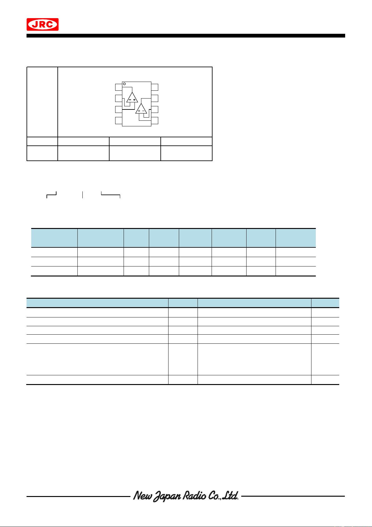
●Package Outline DMP8, SSOP8,
MSOP8 (TVSP8)*
*meet JEDEC MO-187-DA / thin type
APPLICATIONS
●Portable Audio
●PC Audio
●AD/DA Converter Buffer
●Active Filter
DESCRIPTION
The NJM2740 is a dual low saturation output operational
amplifier featuring low noise of 6.5nV/√Hz.
It can be used both single supply and dual supply, by using
proper bias voltage.
Low operating voltage single 2.2V to 7V or dual ±1.1V to
±3.5V and low saturation output performance makes
NJM2740 suitable for Battery-powered instruments,
portable audio devices that require a low voltage and low
saturation output.
The NJM2740 is available in 8-pin DMP, SSOP and
MSOP(TVSP): meet JEDEC MO-187-DA / thin type
package.
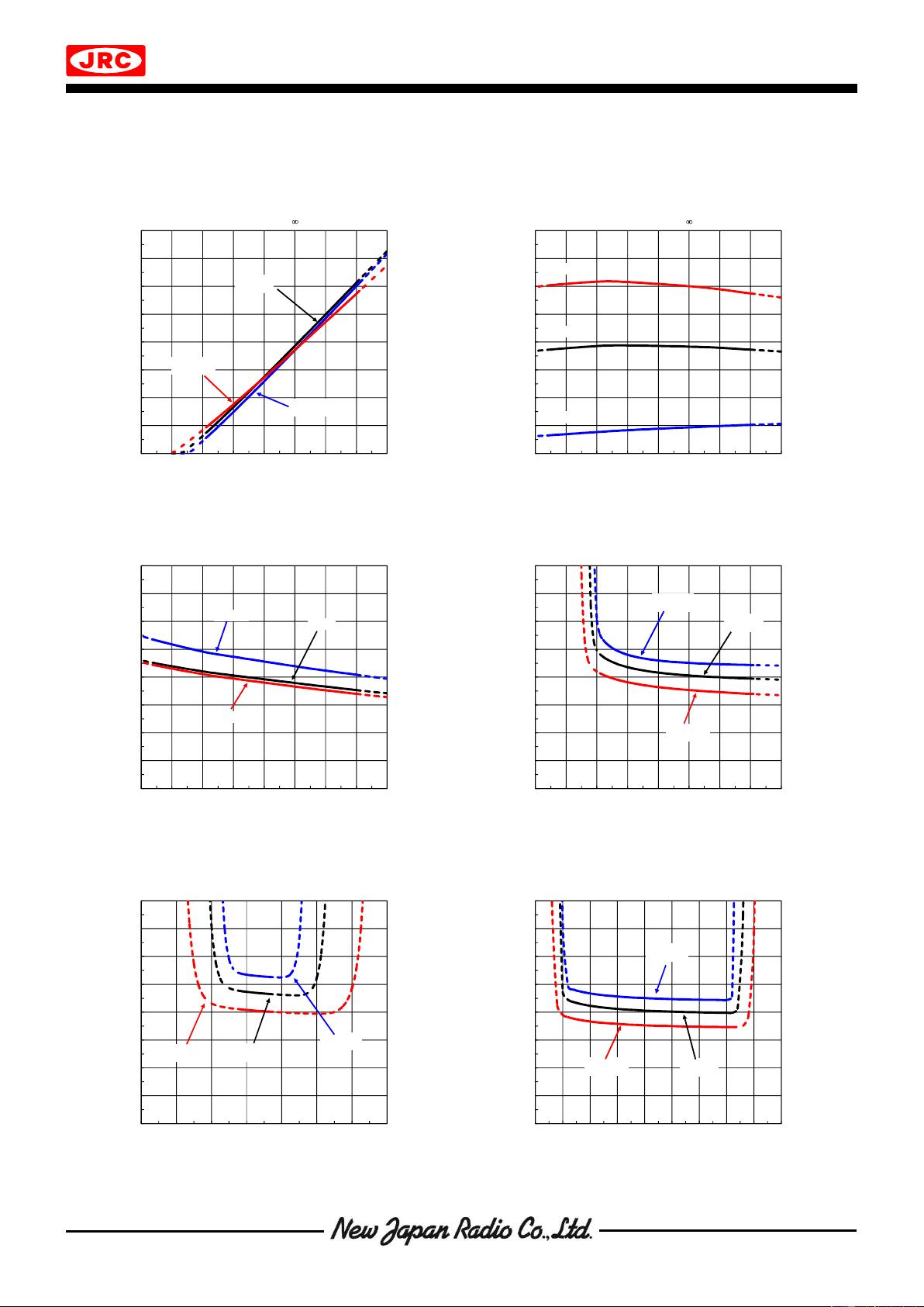
TYPICAL CHARACTERISTICS EQUIVALENT CIRCUIT
0
6
12
18
24
1 10 100 1k 10k 100k
Equivalent Input Noise Voltage [nV/√Hz]
Frequency [Hz]
Voltage Noise Density vs. Frequency
V
+
=5V, Ta=25°C
-

剩余16页未读,继续阅读


评论0
最新资源