没有合适的资源?快使用搜索试试~ 我知道了~
AD7874.pdf
1.该资源内容由用户上传,如若侵权请联系客服进行举报
2.虚拟产品一经售出概不退款(资源遇到问题,请及时私信上传者)
版权申诉
0 下载量 73 浏览量
2024-03-15
11:19:58
上传
评论
收藏 414KB PDF 举报
温馨提示
试读
16页
中国电子设计竞赛,大学生,获奖论文,资料分享,芯片资料,方案参考,
资源推荐
资源详情
资源评论
REV. C
Information furnished by Analog Devices is believed to be accurate and
reliable. However, no responsibility is assumed by Analog Devices for its
use, nor for any infringements of patents or other rights of third parties
which may result from its use. No license is granted by implication or
otherwise under any patent or patent rights of Analog Devices.
a
LC
2
MOS 4-Channel, 12-Bit Simultaneous
Sampling Data Acquisition System
AD7874
One Technology Way, P.O. Box 9106, Norwood, MA 02062-9106, U.S.A.
Tel: 617/329-4700 Fax: 617/326-8703
FUNCTIONAL BLOCK DIAGRAM
AGND
CLK
DGND
DB11
DB0
V
SS
CS
12-BIT
DAC
V
IN1
V
IN2
V
IN3
V
IN4
COMP
REFERENCE
BUFFER
INT
RD
AD7874
CONVST
V
DD
V
DD
REF IN
REF OUT
3V
REFERENCE
DATA
REGISTERS
SAR
MUX
CONTROL LOGIC
INTERNAL
CLOCK
TRACK/
HOLD 3
TRACK/
HOLD 4
TRACK/
HOLD 2
TRACK/
HOLD 1
GENERAL DESCRIPTION
The AD7874 is a four-channel simultaneous sampling, 12-bit
data acquisition system. The part contains a high speed 12-bit
ADC, on-chip reference, on-chip clock and four track/hold am-
plifiers. This latter feature allows the four input channels to be
sampled simultaneously, thus preserving the relative phase
information of the four input channels, which is not possible if
all four channels share a single track/hold amplifier. This makes
the AD7874 ideal for applications such as phased-array sonar
and ac motor controllers where the relative phase information is
important.
The aperture delay of the four track/hold amplifiers is small and
specified with minimum and maximum limits. This allows sev-
eral AD7874s to sample multiple input channels simultaneously
without incurring phase errors between signals connected to
several devices. A reference output/reference input facility also
allows several AD7874s to be driven from the same reference
source.
In addition to the traditional dc accuracy specifications such as
linearity, full-scale and offset errors, the AD7874 is also fully
specified for dynamic performance parameters including distor-
tion and signal-to-noise ratio.
The AD7874 is fabricated in Analog Devices’ Linear Compat-
ible CMOS (LC
2
MOS) process, a mixed technology process
that combines precision bipolar circuits with low-power CMOS
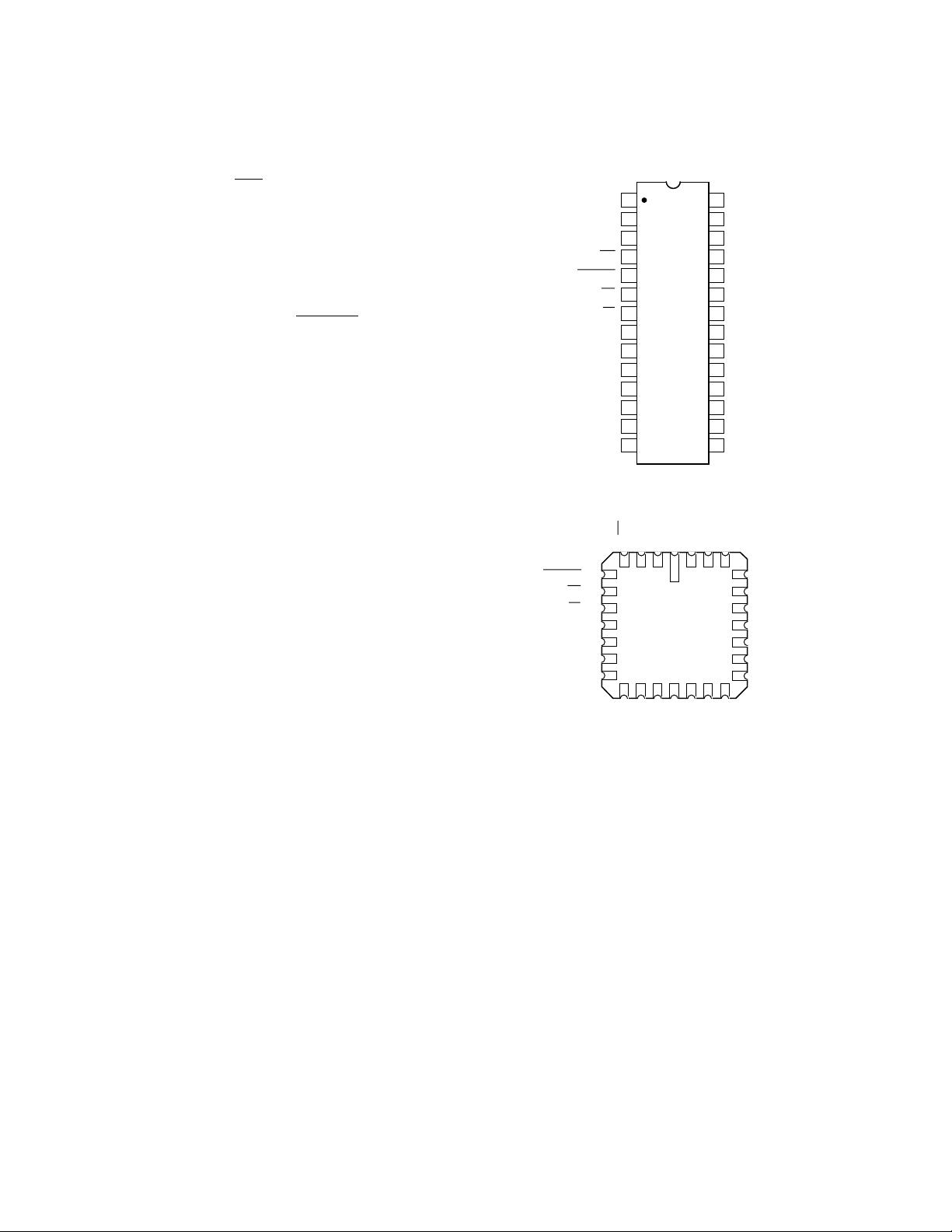
logic. The part is available in a 28-pin, 0.6" wide, plastic or her-
metic dual-in-line package (DIP), in a 28-terminal leadless ce-
ramic chip carrier (LCCC) and in a 28-pin SOIC.
FEATURES
Four On-Chip Track/Hold Amplifiers
Simultaneous Sampling of 4 Channels
Fast 12-Bit ADC with 8 ms Conversion Time/Channel
29 kHz Sample Rate for All Four Channels
On-Chip Reference
610 V Input Range
65 V Supplies
APPLICATIONS
Sonar
Motor Controllers
Adaptive Filters
Digital Signal Processing
PRODUCT HIGHLIGHTS
1. Simultaneous Sampling of Four Input Channels.
Four input channels, each with its own track/hold amplifier,
allow simultaneous sampling of input signals. Track/hold ac-
quisition time is 2 µs, and the conversion time per channel is
8 µs, allowing 29 kHz sample rate for all four channels.
2. Tight Aperture Delay Matching.
The aperture delay for each channel is small and the aperture
delay matching between the four channels is less than 4 ns.
Additionally, the aperture delay specification has upper and
lower limits allowing multiple AD7874s to sample more than
four channels.
3. Fast Microprocessor Interface.
The high speed digital interface of the AD7874 allows direct
connection to all modern 16-bit microprocessors and digital
signal processors.
REV. C
–2–
AD7874–SPECIFICATIONS
(V
DD
= +5 V, V
SS
= –5 V, AGND = DGND = 0 V, REF IN = +3 V, f
CLK
= 2.5 MHz
external. All specifications T
MIN
to T
MAX
unless otherwise noted.)
Parameter A Version B Version S Version Units Test Conditions/Comments
SAMPLE-AND-HOLD
Acquisition Time
2
to 0.01% 2 2 2 µs max
Droop Rate
2, 3
1 1 2 mV/ms max
–3 dB Small Signal Bandwidth
3
500 500 500 kHz typ V
IN
= 500 mV p-p
Aperture Delay
2
0 0 0 ns min
40 40 40 ns max
Aperture Jitter
2, 3
200 200 200 ps typ
Aperture Delay Matching
2
4 4 4 ns max
SAMPLE-AND-HOLD AND ADC
DYNAMIC PERFORMANCE
Signal-to-Noise Ratio 70 71 70 dB min f
IN
= 10 kHz Sine Wave, f
SAMPLE
= 29 kHz
Total Harmonic Distortion –78 –80 –78 dB max f
IN
= 10 kHz Sine Wave, f
SAMPLE
= 29 kHz
Peak Harmonic or Spurious Noise –78 –80 –78 dB max f
IN
= 10 kHz Sine Wave, f
SAMPLE
= 29 kHz
Intermodulation Distortion fa = 9 kHz, fb = 9.5 kHz, f
SAMPLE
= 29 kHz
2nd Order Terms –80 –80 –80 dB max
3rd Order Terms –80 –80 –80 dB max
Channel-to-Channel Isolation
2
–80 –80 –80 dB max
DC ACCURACY
Resolution 12 12 12 Bits
Relative Accuracy ±1 ±1/2 ±1 LSB max
Differential Nonlinearity ±1 ±1 ±1 LSB max No Missing Codes Guaranteed
Positive Full-Scale Error
4
±5 ±5 ±5 LSB max Any Channel
Negative Full-Scale Error
4
±5 ±5 ±5 LSB max Any Channel
Full-Scale Error Match 5 5 5 LSB max Between Channels
Bipolar Zero Error ±5 ±5 ±5 LSB max Any Channel
Bipolar Zero Error Match 4 4 4 LSB max Between Channels
ANALOG INPUTS
Input Voltage Range ±10 ±10 ±10 Volts
Input Current ±600 ±600 ±600 µA max
REFERENCE OUTPUTS
REF OUT 333V nom
REF OUT Error @ +25°C ±0.33 ±0.33 ±0.33 % max
T
MIN
to T
MAX
±1 ±1 ±1 % max
REF OUT Temperature Coefficient ±35 ±35 ±35 ppm/°C typ
Reference Load Change ±1 ±1 ±2 mV max Reference Load Current Change (0–500 µA)
Reference Load Should Not Be Changed During Conversion
REFERENCE INPUT
Input Voltage Range 2.85/3.15 2.85/3.15 2.85/3.15 V min/V max 3 V ± 5%
Input Current ±1 ±1 ±1 µA max
Input Capacitance
3
10 10 10 pF max
LOGIC INPUTS
Input High Voltage, V
INH
2.4 2.4 2.4 V min V
DD
= 5 V ± 5%
Input Low Voltage, V
INL
0.8 0.8 0.8 V max V
DD
= 5 V ± 5%
Input Current, I
IN
±10 ±10 ±10 µA max V
IN
= 0 V to V
DD
Input Capacitance, C
IN
3
10 10 10 pF max
LOGIC OUTPUTS
Output High Voltage, V
OH
4.0 4.0 4.0 V min V
DD
= 5 V ± 5%; I
SOURCE
= 40 µA
Output Low Voltage, V
OL
0.4 0.4 0.4 V max V
DD
= 5 V ± 5%; I
SINK
= 1–6 mA
DB0–DB11
Floating-State Leakage Current ±10 ±10 ±10 µA max V
IN
= 0 V to V
DD
Floating-State Output Capacitance 10 10 10 pF max
Output Coding 2s COMPLEMENT
POWER REQUIREMENTS
V
DD
+5 +5 +5 V nom ±5% for Specified Performance
V
SS
–5 –5 –5 V nom ±5% for Specified Performance
I
DD
18 18 18 mA max CS = RD = CONVST = +5 V; Typically 12 mA
I
SS
12 12 12 mA max CS = RD = CONVST = +5 V; Typically 8 mA
Power Dissipation 150 150 150 mW max CS = RD = CONVST = +5 V; Typically 100 mW
NOTES
1
Temperature ranges are as follows: A, B Versions: –40°C to +85°C; S Version: –55°C to +125°C.
2
See Terminology.
3
Sample tested @ +25°C to ensure compliance.
4
Measured with respect to the REF IN voltage and includes bipolar offset error.
5
For capacitive loads greater than 50 pF a series resistor is required.
Specifications subject to change without notice.
AD7874
REV. C
–3–
TIMING CHARACTERISTICS
1
Parameter A, B Versions S Version Units Conditions/Comments
t
1
50 50 ns min CONVST Pulse Width
t
2
0 0 ns min CS to RD Setup Time
t
3
60 70 ns min RD Pulse Width
t
4
0 0 ns min CS to RD Hold Time
t
5
60 60 ns max RD to INT Delay
t
6
2
57 70 ns max Data Access Time after RD
t
7
3
55ns min Bus Relinquish Time after RD
45 50 ns max
t
8
130 150 ns min Delay Time between Reads
t
CONV
31 31 µs min CONVST to INT, External Clock
32.5 32.5 µs max
CONVST to INT, External Clock
31 31 µs min
CONVST to INT, Internal Clock
35 35 µs max
CONVST to INT, Internal Clock
t
CLK
10 10 µs max Minimum Input Clock Period
NOTES
1
Timing Specifications in bold print are 100% production tested. All other times are sample tested at +25°C to ensure compliance. All input signals are specified with
tr = tf = 5 ns (10% to 90% of +5 V) and timed from a voltage level of 1.6 V.
2
t
6
is measured with the load circuit of Figure 1 and defined as the time required for an output to cross 0.8 V or 2.4 V.
3
t
7
is derived from the measured time taken by the data outputs to change 0.5 V when loaded with the circuit of Figure 2. The measured number is then extrapolated
back to remove the effects of charging or discharging the 50 pF capacitor. This means that the time, t
7
, quoted in the timing characteristics is the true bus relinquish
time of the part and as such is independent of external bus loading capacitances.
Specifications subject to change without notice.
(V
DD
= +5 V 6 5%, V
SS
= –5 V 6 5%, AGND = DGND = O V, t
CLK
= 2.5 MHz external unless
otherwise noted.)
ABSOLUTE MAXIMUM RATINGS*
(T
A
= +25°C unless otherwise noted)
V
DD
to AGND . . . . . . . . . . . . . . . . . . . . . . . . . –0.3 V to +7 V
V
DD
to DGND . . . . . . . . . . . . . . . . . . . . . . . . . –0.3 V to +7 V
V
SS
to AGND . . . . . . . . . . . . . . . . . . . . . . . . . +0.3 V to –7 V
AGND to DGND . . . . . . . . . . . . . . . . –0.3 V to V
DD
+ 0.3 V
V
IN
to AGND . . . . . . . . . . . . . . . . . . . . . . . . .–15 V to +15 V
REF OUT to AGND . . . . . . . . . . . . . . . . . . . . . . . 0 V to V
DD
Digital Inputs to DGND . . . . . . . . . . . –0.3 V to V
DD
+ 0.3 V
Digital Outputs to DGND . . . . . . . . . . –0.3 V to V
DD
+ 0.3 V
Operating Temperature Range
Commercial (A, B Versions) . . . . . . . . . . . –40°C to +85°C
Extended (S Version) . . . . . . . . . . . . . . . . –55°C to +125°C
Storage Temperature Range . . . . . . . . . . . . –65°C to +150°C
Lead Temperature (Soldering, 10 secs) . . . . . . . . . . . +300°C
Power Dissipation (Any Package) to +75°C . . . . . . 1,000 mW
Derates above +75°C by . . . . . . . . . . . . . . . . . . . . 10 mW/°C
*Stresses above those listed under “Absolute Maximum Ratings” may cause
permanent damage to the device. This is a stress rating only and functional
operation of the device at these or any other conditions above those listed in the
operational sections of this specifications is not implied. Exposure to absolute
maximum rating conditions for extended periods may affect device reliability.
TO OUTPUT
PIN
1.6mA
2.1V+
200µA
50pF
Figure 1. Load Circuit for Access Time
TO OUTPUT
PIN
1.6mA
2.1V+
200µA
50pF
Figure 2. Load Circuit for Bus Relinquish Time
WARNING!
ESD SENSITIVE DEVICE
CAUTION
ESD (electrostatic discharge) sensitive device. Electrostatic charges as high as 4000 V readily
accumulate on the human body and test equipment and can discharge without detection.
Although the AD7874 features proprietary ESD protection circuitry, permanent damage may
occur on devices subjected to high energy electrostatic discharges. Therefore, proper ESD
precautions are recommended to avoid performance degradation or loss of functionality.
AD7874
REV. C
–4–
TERMINOLOGY
ACQUISITION TIME
Acquisition Time is the time required for the output of the
track/hold amplifiers to reach their final values, within ±1/2
LSB, after the falling edge of
INT (the point at which the track/
holds return to track mode). This includes switch delay time,
slewing time and settling time for a full-scale voltage change.
APERTURE DELAY
Aperture Delay is defined as the time required by the internal
switches to disconnect the hold capacitors from the inputs. This
produces an effective delay in sample timing. It is measured by
applying a step input and adjusting the
CONVST input position
until the output code follows the step input change.
APERTURE DELAY MATCHING
Aperture Delay Matching is the maximum deviation in aperture
delays across the four on-chip track/hold amplifiers.
APERTURE JITTER
Aperture Jitter is the uncertainty in aperture delay caused by
internal noise and variation of switching thresholds with signal
level.
DROOP RATE
Droop Rate is the change in the held analog voltage resulting
from leakage currents.
CHANNEL-TO-CHANNEL ISOLATION
Channel-to-Channel Isolation is a measure of the level of
crosstalk between channels. It is measured by applying a full-
scale 1 kHz signal to the other three inputs. The figure given is
the worst case across all four channels.
SNR, THD, IMD
See DYNAMIC SPECIFICATIONS section.
PIN CONFIGURATIONS
DIP and SOIC
V
IN1
V
IN2
V
IN4
V
IN3
REF IN
AGND
DB0 (LSB)
V
DD
V
SS
REF OUT
CLK DB1
V
DD
DB2
DB11 (MSB) DB3
DB10 DB4
DB9 DB5
DB8 DB6
DGND DB7
13
18
1
2
28
27
5
6
7
24
23
22
3
4
26
25
821
920
10
19
1111
12
17
16
14
15
TOP VIEW
(Not to Scale)
AD7874
INT
CONVST
RD
CS
LCCC
V
DD
CLK
V
DD
V
IN4
V
IN2
V
IN1
DB9
DB8
DB6
DGND
DB7
REF OUT
REF IN
DB1
AGND
DB0 (LSB)
DB10
DB11 (MSB)
DB4
DB5
V
SS
V
IN3
DB3
DB2
AD7874
27
1
2822634
25
22
24
23
21
19
20
181712 13 1614 15
11
10
9
8
7
6
5
TOP VIEW
(Not to Scale)
CONVST
RD
CS
INT
剩余15页未读,继续阅读
资源评论
阿拉伯梳子
- 粉丝: 1651
- 资源: 5735
上传资源 快速赚钱
- 我的内容管理 展开
- 我的资源 快来上传第一个资源
- 我的收益 登录查看自己的收益
- 我的积分 登录查看自己的积分
- 我的C币 登录后查看C币余额
- 我的收藏
- 我的下载
- 下载帮助
安全验证
文档复制为VIP权益,开通VIP直接复制
信息提交成功