

Rev 1.1
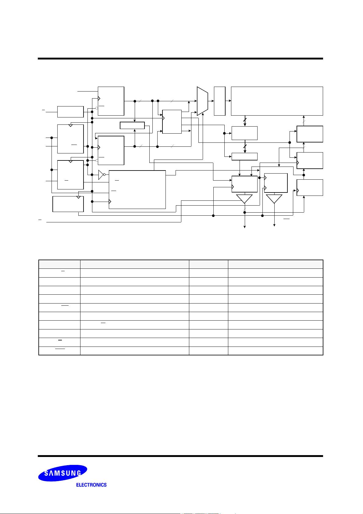
512Kx36 & 1Mx18 SRAM
- 1 -
Jan. 2005
K7D161874B
K7D163674B
Document Title
16M DDR SYNCHRONOUS SRAM
Revision History
The attached data sheets are prepared and approved by SAMSUNG Electronics. SAMSUNG Electronics CO., LTD. reserve the
right to change the specifications. SAMSUNG Electronics will evaluate and reply to your requests and questions on the parameters
of this device. If you have any questions, please contact the SAMSUNG branch office near your office, call or cortact Headquarters.
Rev No.
Rev. 0.0
Rev. 0.1
Rev. 0.2
Rev. 0.3
Rev. 1.0
Rev. 1.1
Remark
Advance
Preliminary
Preliminary
Preliminary
Final
Final
History
Initial document.
Change JTAG DC OPERATING CONDITONS/AC TEST CONDITIONS
-to support 1.8~2.5V V
DD, change some items.
Change DC CHARACTERISTICS (Stop Clock Standby Current)
-I
SB1 : 100 -> 150
Change JTAG Instruction Cording
- For Reserved
Change DC CHARACTERISTICS (Increase Operating Current)
-
x36 : add 40mA, x18 : add 60mA
Add DC CHARACTERISTICS
-
VIN-CLK, VDIF-CLK, VCM-CLK
Add AC INPUT CHARACTERISTICS
Add INPUT DEFINITION
Draft Data
Oct. 2003
Nov. 2003
Feb. 2004
Feb. 2004
Mar. 2004
Jan. 2004
剩余15页未读,继续阅读
资源评论


LC灵灵
- 粉丝: 1
- 资源: 261


最新资源
- 基于C语言的嵌入式软件定时器详细文档+全部资料+高分项目+源码.zip
- 基于ffmpeg的直播推流器,超级稳定,经过长时间稳定性测试,超低延时,可用于手机,电视,嵌入式等直播App及设备。详细文档+全部资料+高分项目+源码.zip
- 基于DCT算法的水印嵌入和提取的移动智能终端数字图像证据系统详细文档+全部资料+高分项目+源码.zip
- 基于FPGA的DDR1控制器,为低端FPGA嵌入式系统提供廉价、大容量的存储详细文档+全部资料+高分项目+源码.zip
- 基于FreeRTOS开发的嵌入式开发框架详细文档+全部资料+高分项目+源码.zip
- 基于FMCW雷达的多天线定位系统详细文档+全部资料+高分项目+源码.zip
- 基于FriendlyARM6410平台的嵌入式Qt程序:实时天气信息,远程vnc控制,远程监视摄像头,语音控制,语音输出TTS详细文档+全部资料+高分项目+源码.zip
- 基于FSMPSTem32的嵌入式音乐播放器、实训作业详细文档+全部资料+高分项目+源码.zip
- 基于GEC6818嵌入式大作业详细文档+全部资料+高分项目+源码.zip
- 基于jetty嵌入式容器的java性能分析工具,内嵌H2 database,以图表形式直观展现应用当前性能数据详细文档+全部资料+高分项目+源码.zip
- 基于jq开发的数学公式插件,可随意嵌入web中详细文档+全部资料+高分项目+源码.zip
- 基于Linux系统的应用程序,旨在搭建一套完整的多进程多线程通讯的消息框架. 支持多SOC的嵌入式APP详细文档+全部资料+高分项目+源码.zip
- 基于mplayer的嵌入式音视频播放器详细文档+全部资料+高分项目+源码.zip
- 基于LSM-Tree的嵌入式数据库详细文档+全部资料+高分项目+源码.zip
- 基于liunx下的一个QT程序,KTV点歌系统嵌入式设备详细文档+全部资料+高分项目+源码.zip
- 基于MySQL的嵌入式Linux智慧农业采集控制系统详细文档+全部资料+高分项目+源码.zip
资源上传下载、课程学习等过程中有任何疑问或建议,欢迎提出宝贵意见哦~我们会及时处理!
点击此处反馈


