没有合适的资源?快使用搜索试试~ 我知道了~
资源推荐
资源详情
资源评论
SC8721 DATASHEET DRAFT
SOUTHCHIP SEMICONDUCTOR SOUTHCHIP CONFIDENTIAL, SUBJECT TO CHANGE
Copyright © 2019, Southchip Semiconductor Technology (Shanghai) Co., Ltd. 1
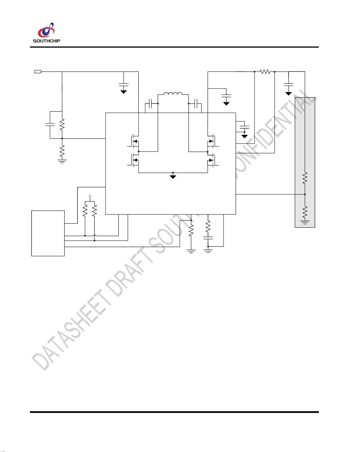
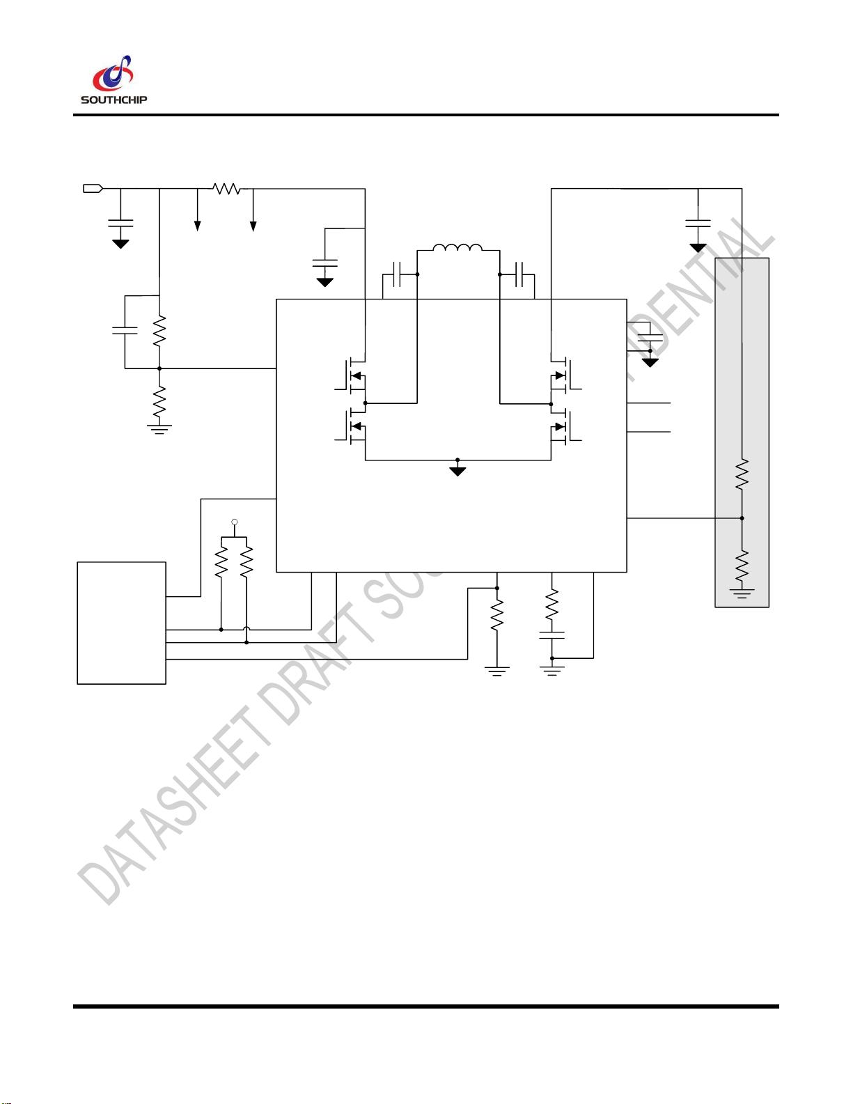
SC8721 High Efficiency, Synchronous, Buck-Boost Converter
with Four Integrated MOSFET
1 Descriptions
SC8721 is a synchronous 4-switch buck-boost converter
with four integrated switches. It is able to effectively output
voltage no matter it is higher, lower or equal to the input
voltage.
SC8721 supports very wide input and output voltage range.
It can support applications from 2.7V to 22V input range and
2.7V to 22V output range. Through its I2C interface, user
can program the output voltage and output current limit and
switching frequency. VINREG voltage can be adjusted by
external resistor.
SC8721 employs current-mode control and supports output
current limit, dynamic output voltage adjustment, internal
current limit, output short protection and over temperature
protections to ensure safety under different abnormal
conditions.
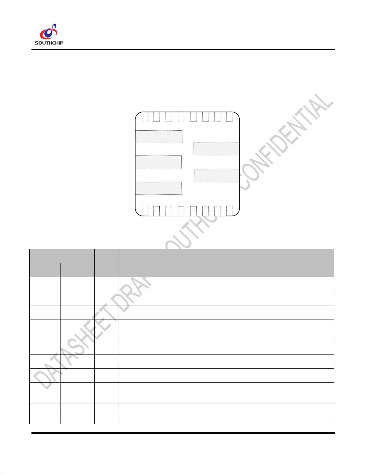
The IC is in a 21 pin 4x4 QFN package.
2 Features
• High Efficiency Buck-Boost Conversion
• Integrated Switches, 10 mΩ for Q1/4, 20 mΩ for Q2/3
• Wide VIN Range: 2.7 V to 22 V, 25V sustainable
• Wide VOUT Range: 2.7 V to 22 V, 25V sustainable
• Dynamic Output Voltage Control
• Adjustable Switching Frequency
• Output Voltage Cable Drop Compensation
• I2C Programmable Output Voltage
• I2C Programmable Output Current Limit
• Output Current Monitor
• Under Voltage Protection, Over Voltage Protection,
Over Current Protection
• Short Protection
• Thermal Shutdown Protection
• QFN-21 4 x 4 Package
3 Applications
• USB Power Delivery
• Wall Adapter
• Type C Hub
• Industry Power Supplies
4 Device Information
Part Number
Package
Dimension
SC8721QFER
21 pin QFN
4.0mm x 4.0mm x 0.75mm
SC8721 DATASHEET DRAFT
SOUTHCHIP SEMICONDUCTOR SOUTHCHIP CONFIDENTIAL, SUBJECT TO CHANGE
Copyright © 2019, Southchip Semiconductor Technology (Shanghai) Co., Ltd. 2
5 Typical Application Circuit
FB
AGND
COMP
CE
BT1
VSET
VCC
PGND
SW1
VIN
VOUT
VIN
VOUT
BT2
SW2
VDD
Host
Control
SDA
SCL
CSO
Rs
Optional
CSN
CSP
Typical application circuit 1. current sense at VOUT
SC8721 DATASHEET DRAFT
SOUTHCHIP SEMICONDUCTOR SOUTHCHIP CONFIDENTIAL, SUBJECT TO CHANGE
Copyright © 2019, Southchip Semiconductor Technology (Shanghai) Co., Ltd. 3
FB
AGND
COMP
CE
BT1
VSET
VCC
PGND
SW1
VIN
VOUT
VIN
VOUT
BT2
SW2
VDD
Host
Control
SDA
SCL
CSO
Rs
Optional
CSP
CSN
CSP
CSN
CSN
CSP
Typical application circuit 2. current sense at VIN
Note: User can place current sense resistor at VIN or VOUT according to application requirement. SC8721 constantly regulates the sense
resistor current at setting value, which is decided by internal register and CSO resistor. Please refer to Output Current Limit for current
setting specification.
SC8721 DATASHEET DRAFT
SOUTHCHIP SEMICONDUCTOR SOUTHCHIP CONFIDENTIAL, SUBJECT TO CHANGE
Copyright © 2019, Southchip Semiconductor Technology (Shanghai) Co., Ltd. 4
6 Terminal Configuration and Functions
Top View
10
NC
CSO
19
PGND 2
VIN 3
AGND
16
CSN
20
VOUT 1
FB 18
VOUT
SW1
VIN
SW2
PGND
COMP
17
NC 15
7 NC
6 SCL
8 VSET
9 VCC
5 SDA
13 SW2
12 SW1
4 CE
11
BT1
BT2 14
CSP
21
TERMINAL
I/O
DESCRIPTION
NUMBER
NAME
1
VOUT
I/O
The power output node of the converter.
2
PGND
I/O
Power ground. User shall connect PGND and AGND together on PCB.
3
VIN
I/O
the power input node of the converter.
4
CE
I
Chip enable pin, active high: pull this pin to logic low to disable the chip. This pin is internally
pulled high.
5
SDA
I/O
I2C interface data. Connect SDA to the logic rail through a pull up resistor (typical 10 kΩ).
6
SCL
I
I2C interface clock. Connect SCL to the logic rail through a pull up resistor (typical 10 kΩ).
7
NC
Must be floating
8
VSET
IO
VINREG internal 1.2V voltage reference. Set the VINREG voltage by resistor divider from to this
pin
9
VCC
O
Output of an internal regulator. Connect a 2.2 µF ceramic capacitor from VCC to PGND pin close
to the IC. The regulator provides supply for internal gate drivers.
SC8721 DATASHEET DRAFT
SOUTHCHIP SEMICONDUCTOR SOUTHCHIP CONFIDENTIAL, SUBJECT TO CHANGE
Copyright © 2019, Southchip Semiconductor Technology (Shanghai) Co., Ltd. 5
10
NC
Must be floating
11
BT1
I
Connect a 100nF ceramic capacitor between BT1 pin and SW1 pin to provide the boosted bias
voltage for high side gate driver.
12
SW1
I/O
Switching Node 1. Connect to inductor.
13
SW2
I/O
Switching Node 2. Connect to inductor.
14
BT2
I
Connect a 100nF ceramic capacitor between BT2 pin and SW2 pin to provide the boosted bias
voltage for high side gate driver.
15
NC
16
AGND
I/O
Analog ground. User shall connect PGND and AGND together on PCB.
17
COMP
I
Connect a RC network to compensate the control loop.
18
FB
I
Feedback node of VOUT output voltage. Set the VOUT output voltage by the resistor divider
connected at this pin.
19
CSO
O
Use this pin to monitor the current sensed by CSP and CSN pin. The voltage of CSO is
proportional to the sense current.
20
CSN
I
Negative input of an internal current sense amplifier. Connect a current sense resistor (typical 10
mΩ) between CSP and CSN to sense the current.
21
CSP
I
Positive input of an internal current sense amplifier. Connect a current sense resistor (typical 10
mΩ) between CSP and CSN to sense the current.
剩余21页未读,继续阅读
资源评论
Chen...
- 粉丝: 33
- 资源: 32
上传资源 快速赚钱
- 我的内容管理 展开
- 我的资源 快来上传第一个资源
- 我的收益 登录查看自己的收益
- 我的积分 登录查看自己的积分
- 我的C币 登录后查看C币余额
- 我的收藏
- 我的下载
- 下载帮助
安全验证
文档复制为VIP权益,开通VIP直接复制
信息提交成功