MOSFET详解.pdf
172 浏览量
2023-02-20
10:33:36
上传
评论
收藏 647KB PDF 举报


10-2-23 下午1:57MOSFET - Wikipedia, the free encyclopedia
Page 1 of 22http://en.wikipedia.org/wiki/MOSFET
MOSFET
Two power MOSFETs in the surface-
mount package D2PAK. Operating as
switches, each of these components can
sustain a blocking voltage of 120 volts in
the OFF state, and can conduct a
continuous current of 30 amperes in the
ON state, dissipating up to about 100
watts and controlling a load of over 2000
watts. A matchstick is pictured for scale.
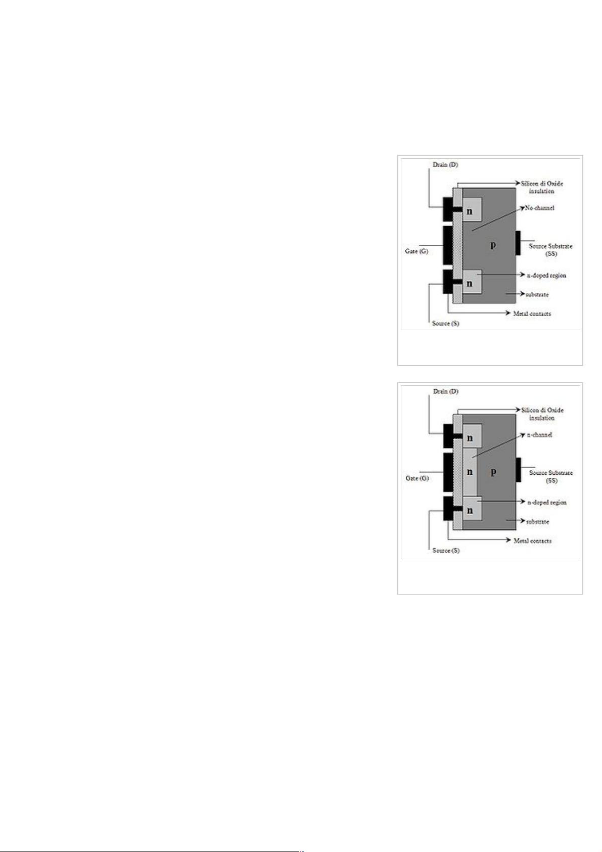
A cross section through an nMOSFET
when the gate voltage V
GS
is below the
threshold for making a conductive
channel; there is little or no conduction
between the terminals source and drain;
the switch is off. When the gate is more
positive, it attracts electrons, inducing an
n-type conductive channel in the substrate
below the oxide, which allows electrons to
flow between the n-doped terminals; the
switch is on.
From Wikipedia, the free encyclopedia
The metal–oxide–semiconductor field-effect transistor
(MOSFET, MOS-FET, or MOS FET) is a device used for
amplifying or switching electronic signals. The basic principle
of the device was first proposed by Julius Edgar Lilienfeld in
1925. In MOSFETs, a voltage on the oxide-insulated gate
electrode can induce a conducting channel between the two
other contacts called source and drain. The channel can be of n-
type or p-type (see article on semiconductor devices), and is
accordingly called an NMOSFET or a PMOSFET (also
commonly nMOS, pMOS). It is by far the most common
transistor in both digital and analog circuits, though the bipolar
junction transistor was at one time much more common.
The 'metal' in the name is now often a misnomer because the
previously metal gate material is now often a layer of
polysilicon (polycrystalline silicon). Aluminium had been the
gate material until the mid 1970s, when polysilicon became
dominant, due to its capability to form self-aligned gates.
Metallic gates are regaining popularity, since it is difficult to
increase the speed of operation of transistors without metal
gates.
IGFET is a related term meaning insulated-gate field-effect
transistor, and is almost synonymous with MOSFET, though it
can refer to FETs with a gate insulator that is not oxide.
Another synonym is MISFET for metal–insulator–
semiconductor FET.
Contents
1 Composition
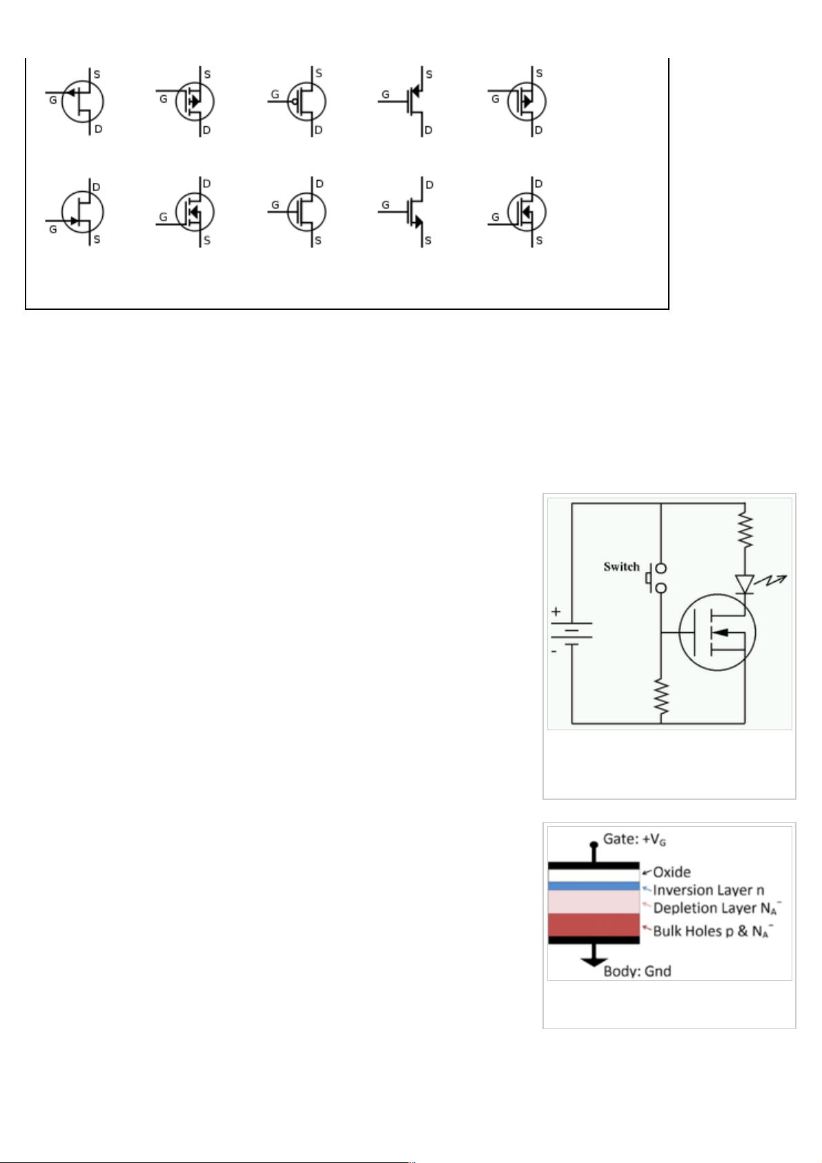
2 Circuit symbols
3 MOSFET operation
3.1 Metal–oxide–semiconductor structure
3.2 MOSFET structure and channel formation
3.3 Modes of operation
3.4 Body effect
剩余21页未读,继续阅读
资源评论


