AR0220-D-1381938.pdf
需积分: 5 11 浏览量
2024-03-15
18:21:02
上传
评论
收藏 452KB PDF 举报

© Semiconductor Components Industries, LLC, 2016
June, 2018 − Rev. 2
1 Publication Order Number:
AR0220/D
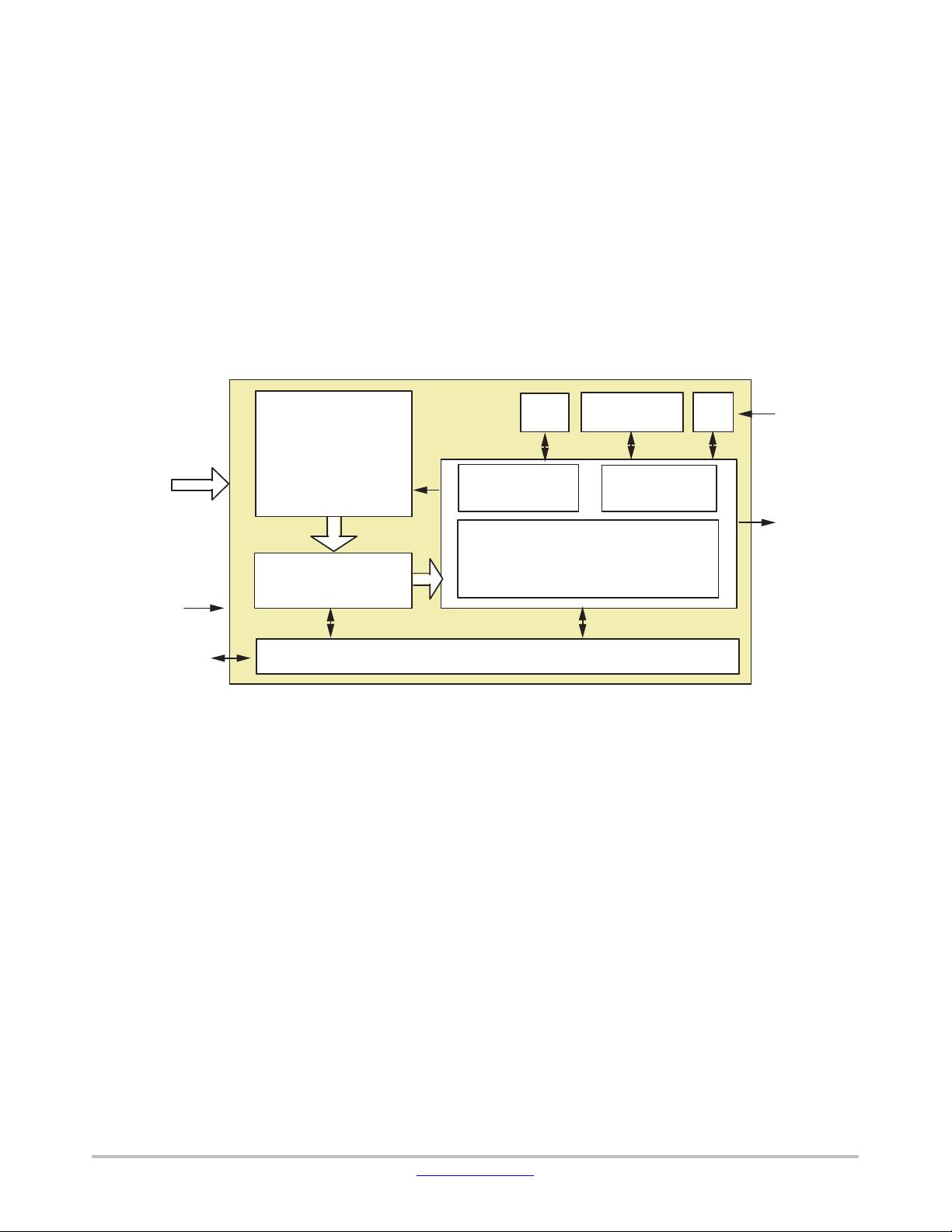
AR0220
1/1.8-Inch CMOS Digital
Image Sensor
General Description
ON Semiconductor AR0220AT is a 1/1.8−inch CMOS digital image
sensor with a 1828 H x 948 V active−pixel array. This advanced
automotive sensor captures images in either linear, or high dynamic
range, with rolling−shutter readout. AR0220AT is optimized for both
low light and challenging high dynamic range scene performance,
with a 4.2 mm BSI pixel and on−sensor 120 dB HDR capture
capability. The sensor includes flexible functions such as in−pixel
binning, windowing, and both video and single frame modes. The
sophisticated sensor fault detection features and embedded data on
AR0220AT are designed to enable camera ASIL B compliance. The
device is programmable through a simple two−wire serial interface,
and supports MIPI output interface.
Table 1. KEY PARAMETERS
Parameter Typical Value
Optical format 1/1.8 inch (8.93 mm)
Active pixels 1820 x 940 = 1.7M
Pixel size
4.2 mm
Color filter array RGB Bayer, RCCC, RCCB
Shutter type Electronic rolling shutter
Input clock range 6 − 50 MHz
Output clock maximum 85.5 MHz
Output Serial MIPI CSI−2 12−, 14−, 16−, or 20−bit
Frame rate Full resolution 60 fps at 3−exposure HDR
36 fps at 4−exposure HDR
Responsivity*
RCCC (Clear) 135 ke−/lux*sec
RGB (Green) 60.5 ke−/lux*sec
RCCB (Clear) 135 ke−/lux*sec
SNR
MAX
44.7 dB
Maximum dynamic range > 120 dB
Supply voltage
I/O 1.8 or 2.8 V
Digital 1.2 V
Analog 2.8 V
MIPI 1.2 V
Power consumption (typical) 424 mW (Full resolution 60 fps MIPI
4 lane output 3−exp HDR mode)
269 mW (Full resolution 60 fps MIPI
4 lane output Linear mode)
Operating temperature −40°C to +105°C (ambient)
−40°C to +125°C (junction)
Package options 12 x 9 mm iBGA
*D65, 670 nm IRCF
Features
• High Performance 4.2 mm Automotive
Grade Backside Illuminated (BSI) Pixel
with DR−Pixt Technology
• Advanced On−Sensor HDR Reconstruct
with Flexible Exposure Ratio Control
• Full Resolution Video Capture at 60fps in
3−exposure HDR and 36fps in 4−exposure
HDR
• Fast Single Exposure Video Capture at
100fps in 10−bit and 85fps in 12−bit output
• Line interleaved T1/T2/T3/T4 output
• Sensor Fault Detection for ASIL−B Com-
pliance Support
• 2x2 In−pixel Binning Mode and Color Bin-
ning Mode
• Data Interfaces: 4−lane MIPI CSI−2
• Selectable Automatic or User Controlled
Black Level Control
• Frame to Frame Switching Among up to 4
Contexts to Enable Multi−function Systems
• Spread−spectrum Input Clock Support
• Multi−Camera Synchronization Support
• Multiple CFA Options including RGB, and
RCCC, RCCB
• These are Pb−Free Devices
www.onsemi.com
This document, and the information contained herein,
is CONFIDENTIAL AND PROPRIETARY and the
property of Semiconductor Components Industries,
LLC., dba ON Semiconductor. It shall not be used,
published, disclosed or disseminated outside of the
Company, in whole or in part, without the written
permission of ON Semiconductor. Reverse
engineering of any or all of the information contained
herein is strictly prohibited.
E 2018, SCILLC. All Rights Reserved.


剩余25页未读,继续阅读
资源评论


