没有合适的资源?快使用搜索试试~ 我知道了~
Si446x 无线模块PCB设计指导
4星 · 超过85%的资源 需积分: 10 10 下载量 109 浏览量
2016-09-01
16:25:16
上传
评论
收藏 3.3MB PDF 举报
温馨提示
试读
32页
Si4460/61/63/64/67/68 RF ICs Layout Design Guide
资源推荐
资源详情
资源评论
Rev. 0.3 Copyright © 2014 by Silicon Laboratories AN629
AN629
Si4460/61/63/64/67/68 RF ICs Layout Design Guide
1. Introduction
The purpose of this application note is to help users design PCBs for the next generation EZRadioPRO™ RF ICs,
i.e. the Si4460/61/63/64/67/68 devices (henceforth referred to as EZRadioPRO™ RF ICs) using good design
practices that allow for good RF performance. The matching principles described in detail in “AN627: Si4460/61/67
Low-Power PA Matching” and in “AN648: Si4063/Si4463/64/68 TX Matching”.
The RF performance and the critical maximum peak voltage on the output pin strongly depend on the PCB layout
as well as the design of the matching networks. For optimal performance, Silicon Labs recommends the use of the
PCB layout design hints described in the following sections.
2. Design Recommendations when Using Si4460/61/63/64/67/68 RF ICs
Extensive testing has been completed using reference designs provided by Silicon Labs. It is
recommended that designers use the reference designs “as-is” since they minimize detuning effects
caused by parasitics or generated by poor component placement and PCB routing.
The compact RF part of the designs is highlighted by a silkscreen frame, and it is strongly recommended to
use the same framed RF layout in order to avoid any possibility of detuning effects. Figure 1 shows the
framed compact RF part of the designs.
Figure 1. Compact RF Part of the Designs Highlighted on Top Silkscreen
When layouts cannot be followed as shown by the reference designs (due to PCB size and shape
limitations), the layout design rules described in the following sections are recommended.
AN629
2 Rev. 0.3
2.1. Matching Network Types and Layout Topologies for the Si4460/61/63/64/67/68 RF ICs
The Si4460/61/63/64/67/68 devices can use the following TX matching networks:
Class E (CLE)
Switched Current (SWC)
Square-Wave (SQW)
The basic types of board layout configurations are as follows:
Split TX/RX
Direct Tie
Switched TX/RX
Diversity
In the Split TX/RX type, the TX and RX paths are separated, and individual SMA connectors are provided for each
path. This type of Pico Board is best suited to demonstrations of the output power and sensitivity of the
EZRadioPRO™ RF ICs.
In the Direct Tie type, the TX and RX paths are connected together directly, without any additional RF switch.
In the Switched TX/RX type, the boards contain a single antenna and a single-pole double-throw (SPDT) RF switch
to select between the TX and RX paths.
In the Diversity type, there are two antennas, both of which can be connected either to the TX or the RX path by a
double-pole double-throw (DPDT) RF switch.
AN629
Rev. 0.3 3
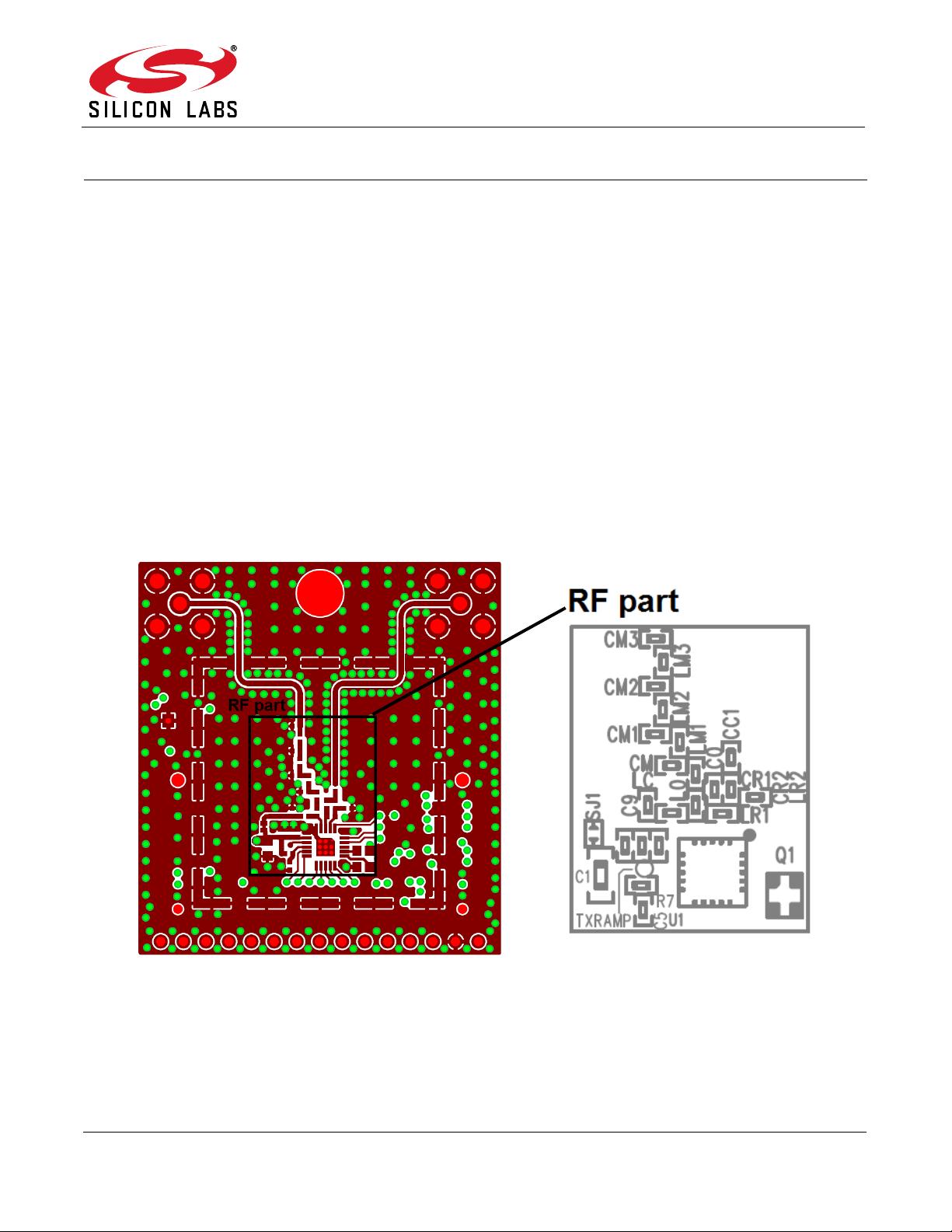
3. Guidelines for Layout Design When Using the Si4460/61/63/64/67/68 RF
ICs in Pico Board Form
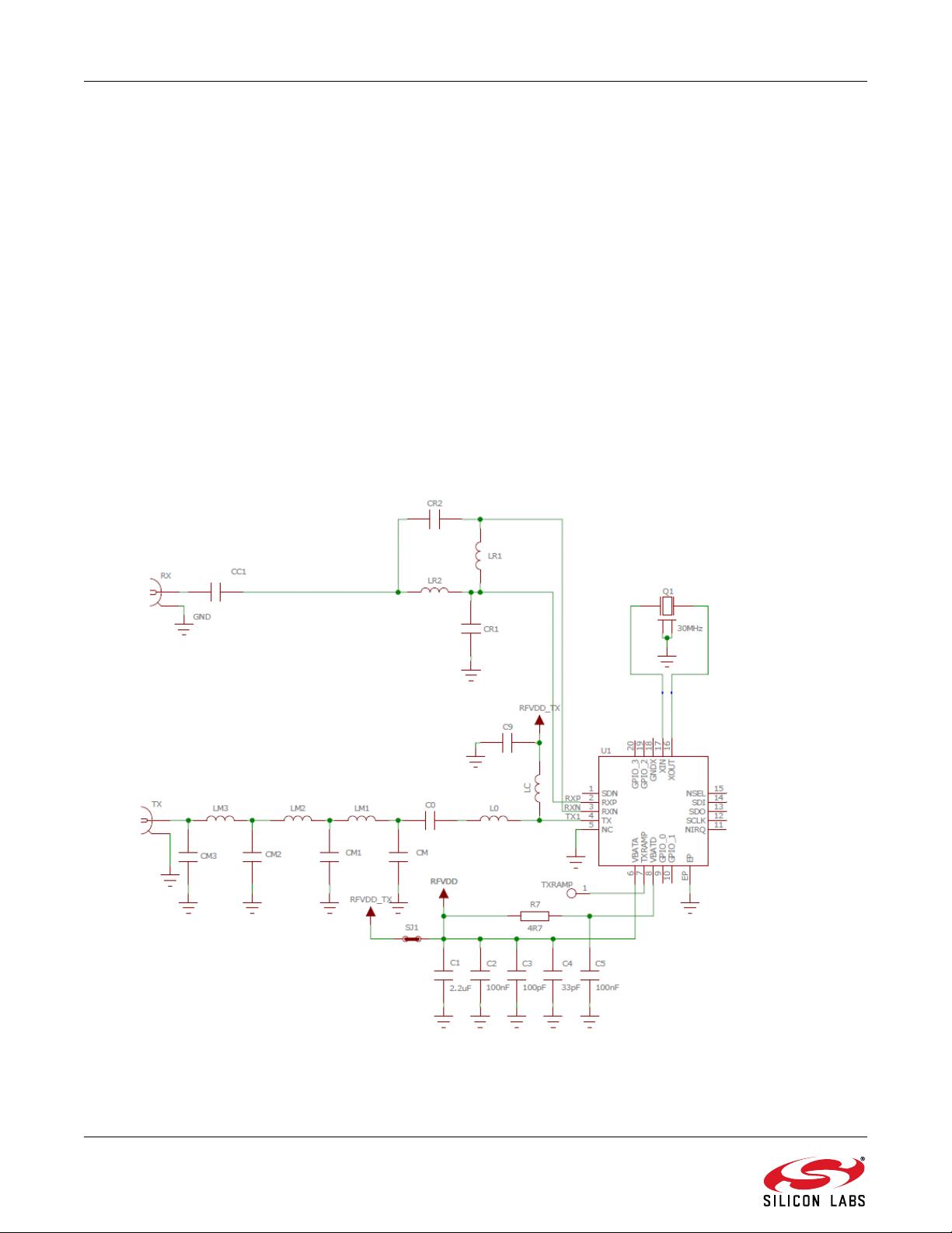
The typical power regime of the Si4461 is in the +13 to +16 dBm range, while the Si4460/67 is primarily devoted to
the +10…+13dBm applications. For these devices, the preferred matching types for the 315 to 950 MHz frequency
range are the CLE and the SWC. The operating principles of these types and the reference designs with element
values are given in “AN627: Si4460/61/67 Low-Power PA Matching”.
For the versions of RF Pico Boards using the Si4463/64/68 RF ICs (i.e., +20 dBm PA) with CLE and SWC type
Split TX/RX and Direct Tie type matchings, general layout guidelines similar to those of the Si4460/61/67 RF ICs
(i.e., +10...+16 dBm PA) can be applied. However, some small additional amount of filtering might be necessary
depending on the harmonic restrictions of the relevant EMC regulation. The layout issues of the SQW type
matching will be discussed in this section as well. This type of matching can be used effectively when the required
output power is high and the operating frequency is low (e.g. 169 MHz). The operating principles of these types
and the reference designs with element values are given in “AN648: Si4063/Si4463/64/68 TX Matching”.
It is not surprising that the increased TX output power of the Si4463/64/68 chips is accompanied by a
corresponding increase in the absolute level of harmonic signals. Since most regulatory standards (e.g. FCC,
ETSI, ARIB etc.) require the harmonic signals to be attenuated below some absolute power level (in watts or
dBm), the amount of low-pass filtering required is generally greater on an RF Pico Board using an Si4463/64/68
chip. Thus the RF Pico Board layout for the Si4463/64/68 RF IC may contain a few more components in the L-C
low pass filter.
Furthermore, in the case of SQW type matching, it is necessary to pay closer attention to the shape and amplitude
of the voltage waveform at the TX output pin of the device due to the increase in output power. Silicon Labs
recommends the addition of a harmonic termination circuit (formed by the LH, CH, and RH components) placed in
parallel shunt-to-GND configuration at the input of the low-pass filter. This harmonic termination circuit helps to
maintain the desired voltage waveform at the TX output pin by providing a good impedance termination at very
high harmonic frequencies. Please refer to “AN648: Si4063/Si4463/64/68 TX Matching” for further details on this
subject.
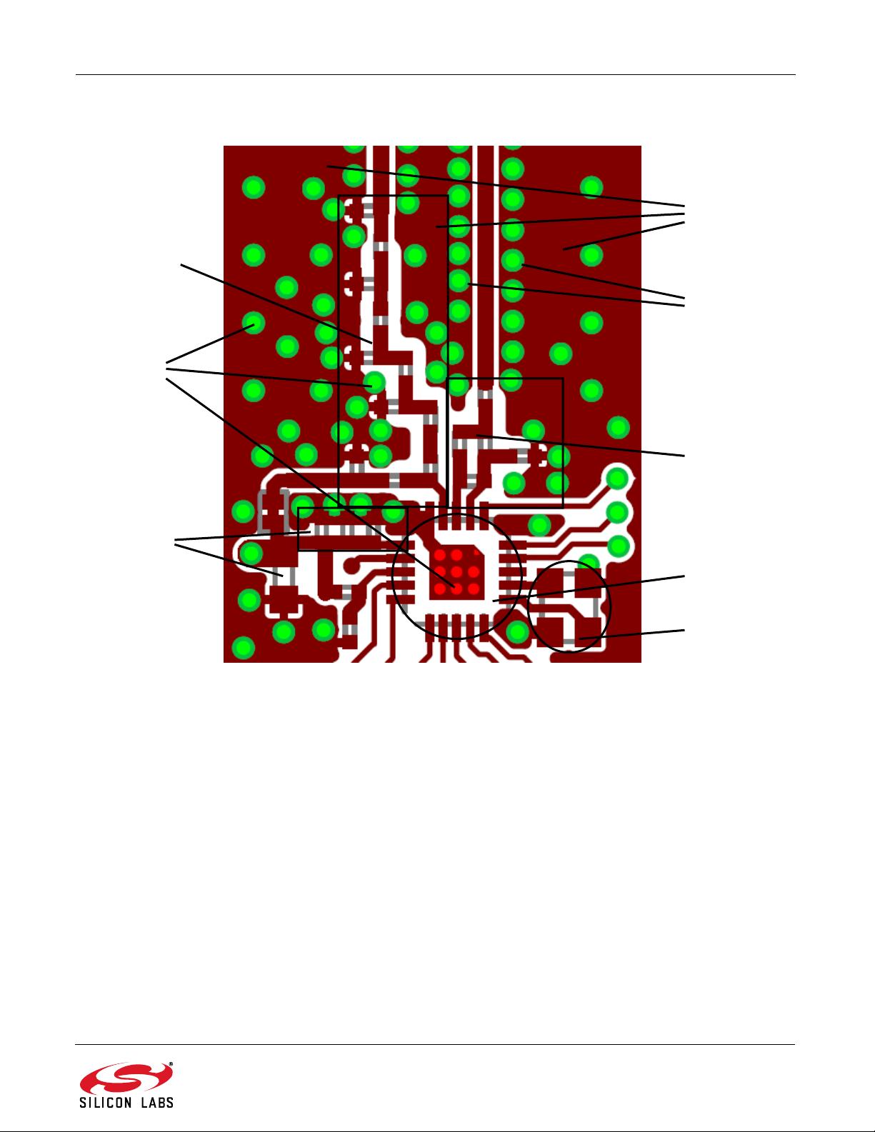
Some general rules of thumb for designing RF-related layouts for good RF performance are:
Use as much continuous ground plane metalization as possible.
Avoid the separation of the ground plane metalization.
Use as many grounding vias (especially near to the GND pins) as possible to minimize series parasitic
inductance between the ground pour and the GND pins.
Use a series of GND vias (a so called “via curtain”) along the PCB edges and internal GND metal pouring
edges. The maximum distance between the vias should be less than lambda/10 of the 10
th
harmonic. This
is required to reduce the PCB radiation at higher harmonics caused by the fringing field of these edges.
Avoid using long and/or thin transmission lines to connect the components. Otherwise, due to its distributed
parasitic inductance some detuning effects can occur.
Try to avoid placing the nearby inductors in the same orientation to reduce the coupling between them.
Use tapered line between transmission lines with different width (i.e. different impedance) to reduce
internal reflections.
Avoid using loops and long wires to obviate its resonances.
Always ensure good V
DD
filtering by using some bypass capacitors (especially at the range of the
operating frequency).
AN629
4 Rev. 0.3
3.1. Class E Split TX/RX Type Matching Network Layout Based on the 4463-PCE20B915
(4463CPCE20B915) Pico Board (Separate TX and RX Paths, with Two Antennas)
Examples shown in this section are mainly based on the layout of the 4463-PCE20B915 Pico Boards which are the
same as 4463CPCE20B915 Pico Boards. These boards contain two separate antennas for the TX and RX paths.
This type of Pico Board is best suited for demonstrating the best possible conducted output power and sensitivity of
the EZRadioPRO™ RF ICs. For this purpose, the layouts of the TX and RX paths are separated and isolated as
much as possible to minimize the coupling effects between them. This type of Pico Board is recommended for
laboratory use and not for range tests since the presence of two closely-spaced antennas may cause “shadowing”
when receiving a radiated signal.
The main layout design concepts are reviewed through this layout to demonstrate the basic principles. However,
for an actual application, the layouts of the Pico Boards with single antenna (or with antenna diversity) should be
used as references.
In this section, a four-layer design (based on the layout of the 4463-PCE20B915 (4463CPCE20B915) Pico Boards)
and a two-layer design (based on the layout of the 4438-PCE20B490 (4438CPCE20B490) Pico Boards) are
shown.
The layout design recommendations for the TX only and RX only Pico Boards are also fully covered in this section
without directly touch these cases.
The schematic of the CLE Split TX/RX type matching network for the Si446x is shown in Figure 2.
Figure 2. Schematic of the CLE Split TX/RX Type Matching Network for the Si446x*
*Note: Component values should be chosen based on frequency band.
AN629
Rev. 0.3 5
The layout structure of the CLE Split TX/RX type matching network is shown in Figure 3.
Figure 3. Schematic of the CLE Split TX/RX Type Matching Network for the Si446x
3.1.1. Layout Design Guidelines
The L0 inductor should be placed as close to the TX pin of the RF IC as possible (even if this means the
RX is further away) in order to reduce the series parasitic inductance which increase the voltage peak at
the internal drain pin.
The TX and RX sections should be separated as much as possible on the top layer to reduce coupling. If
the available space allows, flow the GND metal between them and use many vias.
The neighboring matching network components should be placed as close to each other as possible in
order to minimize any PCB parasitic capacitance to the ground and the series parasitic inductances
between the components.
Improve the grounding effect in the thermal straps used with capacitors. In addition, thicken the trace near
the GND pin of these capacitors. This will minimize series parasitic inductance between the ground pour
and the GND pins. Additional vias placed close to the GND pin of capacitors (thus connecting it to the
bottom layer GND plane) will further help reduce these effects.
Figure 4 demonstrates the positioning and orientation of the LC and LR components, the separating GND metal
between the TX and RX sections, and thermal strapping on the shunt capacitors on the 4463-PCE20B915
(4463CPCE20B915) Pico Boards.
Crystal
RF IC
V
DD
Filter
Capacitors
PCB Vias
TX Section
RX Section
Ground
Metallization
Ground
“Via curtain”
剩余31页未读,继续阅读
资源评论
- wingcky2017-11-18有点用,不错。
zhazhajian1
- 粉丝: 1
- 资源: 2
上传资源 快速赚钱
- 我的内容管理 展开
- 我的资源 快来上传第一个资源
- 我的收益 登录查看自己的收益
- 我的积分 登录查看自己的积分
- 我的C币 登录后查看C币余额
- 我的收藏
- 我的下载
- 下载帮助
安全验证
文档复制为VIP权益,开通VIP直接复制
信息提交成功