没有合适的资源?快使用搜索试试~ 我知道了~
温馨提示
试读
312页
TI dm8168 datasheet The DM816x DaVinci™ Digital Media Processors are a highly-integrated, programmable platform that leverages TI's DaVinci™ technology to meet the processing needs of the following applications: Video Encode/Decode/Transcode/Transrate, Video Security, Video Conferencing, Video Infrastructure, Media Server, and Digital Signage.
资源推荐
资源详情
资源评论
PRODUCTPREVIEW
TMS320DM8168, TMS320DM8167
TMS320DM8166, TMS320DM8165
www.ti.com
SPRS614–MARCH 2011
TMS320DM816x DaVinci
Digital Media Processors
Check for Samples: TMS320DM8168, TMS320DM8167, TMS320DM8166, TMS320DM8165
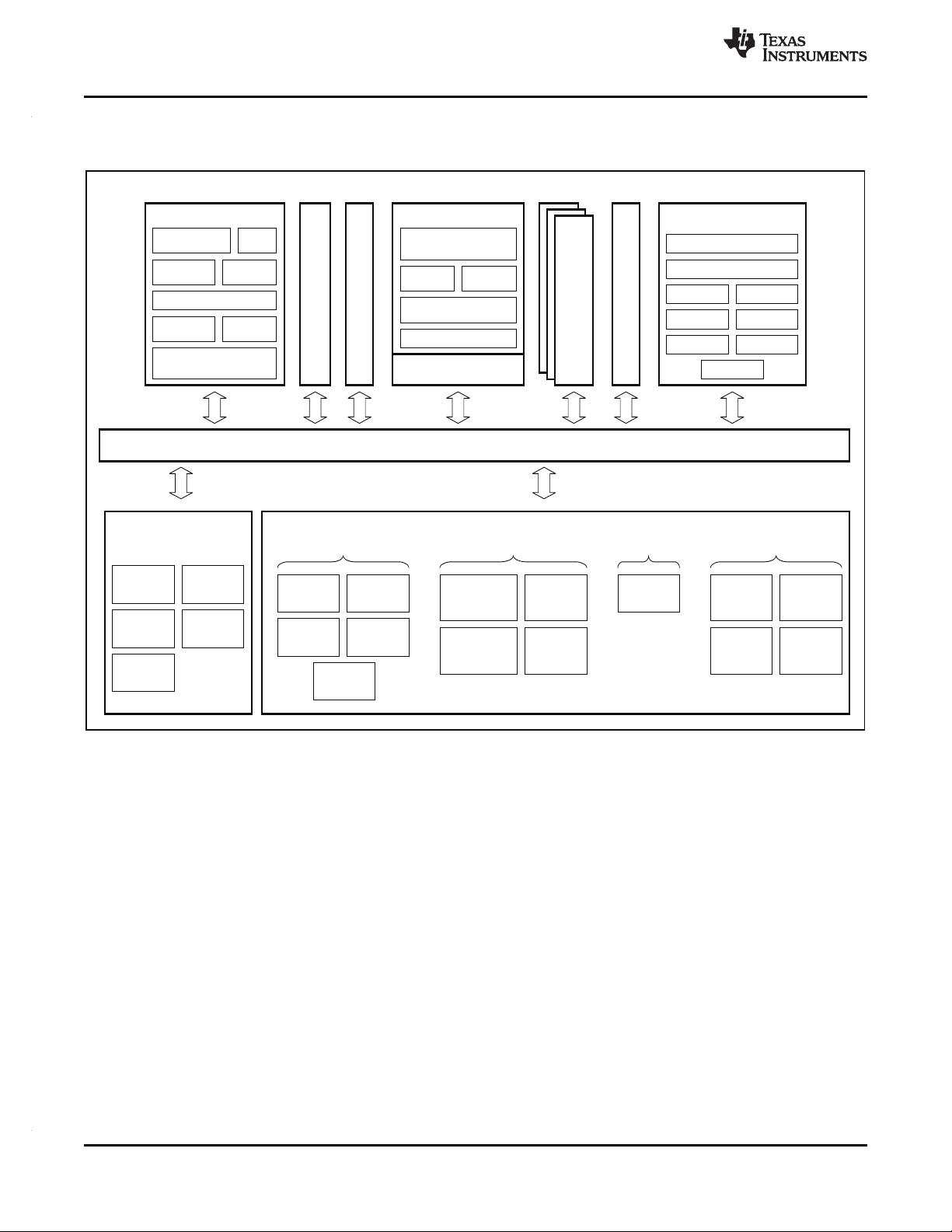
1 Device Summary
1.1 Features
1234567891011
Multiply Supported up to:
• High-Performance DaVinci™ Digital Media
Processors – 2 SP x SP → SP Per Clock
– ARM
®
Cortex™-A8 RISC MPU – 2 SP x SP → DP Every Two Clocks
• Up to 1.2 GHz – 2 SP x DP → DP Every Three Clocks
– C674x VLIW DSP – 2 DP x DP → DP Every Four Clocks
• Up to 1.0 GHz • Fixed-Point Multiply Supports Two 32 x
32 Multiplies, Four 16 x 16-bit Multiplies
• Up to 8000/6000 C674x MIPS/MFLOPS
including Complex Multiplies, or Eight 8 x
• Fully Software-Compatible with C67x+™
8-Bit Multiplies per Clock Cycle
and C64x+™
• C674x Two-Level Memory Architecture
• ARM
®
Cortex™-A8 Core
– 32K-Byte L1P and L1D RAM/Cache
– ARMv7 Architecture
– 256K-Byte L2 Unified Mapped RAM/Caches
• In-Order, Dual-Issue, Superscalar
• DSP/EDMA Memory Management Unit
Microprocessor Core
(DEMMU)
• NEON™ Multimedia Architecture
– Maps C674x DSP and EMDA TCB Memory
– Supports Integer and Floating Point
Accesses to System Addresses
(VFPv3-IEEE754 compliant)
• 512K-Bytes On-Chip Memory Controller
• Jazelle
®
RCT Execution Environment
(OCMC) RAM
• ARM
®
Cortex™-A8 Memory Architecture
• Up to Three Programmable High-Definition
– 32K-Byte Instruction and Data Caches
Video Image Coprocessing (HDVICP2) Engines
– 256K-Byte L2 Cache
– Encode, Decode, Transcode Operations
– 64K-Byte RAM, 48K-Byte Boot ROM
– H.264, MPEG2, VC1, MPEG4 SP/ASP
• TMS320C674x Floating-Point VLIW DSP
• SGX530 3D Graphics Engine (available only on
– 64 General-Purpose Registers (32-Bit)
the DM8168/DM8166 device)
– Six ALU (32-/40-Bit) Functional Units
– Delivers up to 30 MTriangles/s
• Supports 32-Bit Integer, SP (IEEE Single
– Universal Scalable Shader Engine
Precision/32-Bit) and DP (IEEE Double
– Direct3D
®
Mobile, OpenGL
®
ES 1.1 and 2.0,
Precision/64-Bit) Floating Point
OpenVG™ 1.0, OpenMax™ API Support
• Supports up to Four SP Adds Per Clock
– Advanced Geometry DMA Driven Operation
and Four DP Adds Every Two Clocks
– Programmable HQ Image Anti-Aliasing
• Supports up to Two Floating-Point (SP or
• Endianness
DP) Approximate Reciprocal or Square
– ARM/DSP Instructions/Data – Little Endian
Root Operations Per Cycle
• HD Video Processing Subsystem (HDVPSS)
– Two Multiply Functional Units
– Two 165 MHz HD Video Capture Channels
• Mixed-Precision IEEE Floating-Point
1
Please be aware that an important notice concerning availability, standard warranty, and use in critical applications of Texas
Instruments semiconductor products and disclaimers thereto appears at the end of this data sheet.
2DaVinci, C64x+, SmartReflex, TMS320C6000, Code Composer Studio, DSP/BIOS, XDS are trademarks of Texas Instruments.
3Cortex, NEON are trademarks of ARM Ltd or its subsidiaries.
4ARM, Jazelle, Thumb are registered trademarks of ARM Ltd or its subsidiaries.
5USSE, POWERVR are trademarks of Imagination Technologies Limited.
6OpenVG, OpenMax are trademarks of Khronos Group Inc.
7Direct3D, Microsoft, Windows are registered trademarks of Microsoft Corporation in the United States and/or other countries.
8I
2
C BUS is a registered trademark of NXP B.V. Corporation Netherlands.
9PCI Express, PCIe are registered trademarks of PCI-SIG.
10OpenGL is a registered trademark of Silicon Graphics International Corp. or its subsidiaries in the United States and/or other countries.
11All other trademarks are the property of their respective owners.
PRODUCT PREVIEW information concerns products in the formative
Copyright © 2011, Texas Instruments Incorporated
or design phase of development. Characteristic data and other
specifications are design goals. Texas Instruments reserves the right
to change or discontinue these products without notice.
PRODUCTPREVIEW
TMS320DM8168, TMS320DM8167
TMS320DM8166, TMS320DM8165
SPRS614–MARCH 2011
www.ti.com
• One 16/24-bit and One 16-bit Channel – Flexible Asynchronous Protocol Control for
Interface to FPGA, CPLD, ASICs, etc.
• Each Channel Splittable Into Dual 8-bit
Capture Channels • Enhanced Direct-Memory-Access (EDMA)
Controller
– Two 165 MHz HD Video Display Channels
– Four Transfer Controllers
• One 16/24/30-Bit and One 16-bit Channel
– 64/8 Independent DMA/QDMA Channels
– Simultaneous SD and HD Analog Output
• Seven 32-bit General-Purpose Timers
– Digital HDMI 1.3 transmitter with HDCP up to
165-MHz pixel clock • One System Watchdog Timer
– Advanced Video Processing Features Such • Three Configurable UART/IrDA/CIR Modules
as Scan/Format/Rate Conversion
– UART0 With Modem Control Signals
– Three Graphics Layers and Compositors
– Supports up to 3.6864 Mbps UART
• Dual 32-bit DDR2/3 SDRAM Interfaces
– SIR, MIR, FIR (4.0 MBAUD), and CIR
– Supports up to DDR2-800 and DDR3-1600
• One 40-MHz Serial Peripheral Interface (SPI)
– Up to Eight x8 Devices Total With Four Chip-Selects
– 2 GB Total Address Space • SD/SDIO serial interface (1-/4-Bit)
– Dynamic Memory Manager (DMM) • Dual Inter-Integrated Circuit ( I
2
C BUS
®
) Ports
• Programmable Multi-Zone Memory • Three Multichannel Audio Serial Ports
Mapping and Interleaving
– One Six-Serializer Transmit/Receive Port
• Enables Efficient 2D Block Accesses
– Two Dual-Serializer Transmit/Receive Ports
• Supports Tiled Objects in 0°, 90°, 180°, or
– DIT-Capable For S/PDIF (All Ports)
270 Orientation and Mirroring
• Multichannel Buffered Serial Port (McBSP)
• Optimizes Interlaced Accesses
– Transmit/Receive Clocks up to 48 MHz
• One PCI Express
®
(PCIe
®
) 2.0 Port With
– Two Clock Zones and Two Serial Data Pins
Integrated PHY
– Supports TDM, I2S, and Similar Formats
– Single Port With 1 or 2 Lanes at 5.0 GT/s
• Real-Time Clock (RTC)
– Configurable as Root Complex or Endpoint
– One-Time or Periodic Interrupt Generation
• Serial ATA (SATA) 3.0 Gbps Controller With
• Up to 64 General-Purpose I/O (GPIO) Pins
Integrated PHYs
• On-Chip ARM
®
ROM Bootloader (RBL)
– Direct Interface for Two Hard Disk Drives
• Power, Reset, and Clock Management
– Hardware-Assisted Native Command
– SmartReflex™ Technology (Level 2)
Queuing (NCQ) from up to 32 Entries
– Seven Independent Core Power Domains
– Supports Port Multiplier and
– Clock Enable/Disable Control For
Command-Based Switching
Subsystems and Peripherals
• Two 10/100/1000 Mbps Ethernet MACs (EMAC)
• IEEE-1149.1 (JTAG) and IEEE-1149.7 (cJTAG)
– IEEE 802.3 Compliant (3.3V I/O Only)
Compatible
– MII and GMII Media Independent I/Fs
• 1031-Pin Pb-Free BGA Package (CYG Suffix),
– Management Data I/O (MDIO) Module
0.65-mm Ball Pitch
• Dual USB 2.0 Ports With Integrated PHYs
• Via Channel™ Technology Enables use of
– USB 2.0 High-/Full-Speed Client
0.8-mm Design Rules
– USB 2.0 High-/Full-/Low-Speed Host
• 40-nm CMOS Technology
– Supports End Points 0-15
• 3.3-V Single-Ended LVCMOS I/Os (except for
• General Purpose Memory Controller (GPMC)
DDR3 at 1.5 V, DDR2 at 1.8 V, and DEV_CLKIN
– 8-/16-bit Multiplexed Address/Data Bus at 1.8 V)
– Up to 6 Chip Selects With up to 256M-Byte • Applications
Address Space per Chip Select Pin
– Video Encode/Decode/Transcode/Transrate
– Glueless Interface to NOR Flash, NAND
– Video Security
Flash (With BCH and Hamming Error Code
– Video Conferencing
Detection), SRAM and Pseudo-SRAM
– Video Infrastructure
– Error Locator Module (ELM) Outside of
– Media Server
GPMC to Provide Up to 16-Bit/512-Bytes
– Digital Signage
Hardware ECC for NAND
2 Device Summary Copyright © 2011, Texas Instruments Incorporated
Submit Documentation Feedback
Product Folder Link(s): TMS320DM8168 TMS320DM8167 TMS320DM8166 TMS320DM8165
PRODUCTPREVIEW
TMS320DM8168, TMS320DM8167
TMS320DM8166, TMS320DM8165
www.ti.com
SPRS614–MARCH 2011
1.2 Description
The DM816x DaVinci™ Digital Media Processors are a highly-integrated, programmable platform that
leverages TI's DaVinci™ technology to meet the processing needs of the following applications: Video
Encode/Decode/Transcode/Transrate, Video Security, Video Conferencing, Video Infrastructure, Media
Server, and Digital Signage.
The device enables OEMs and ODMs to quickly bring to market devices featuring robust operating
systems support, rich user interfaces, and high processing performance through the maximum flexibility of
a fully integrated mixed processor solution. The device combines programmable video and audio
processing with a highly-integrated peripheral set.
Key to the device are up to three high-definition video/imaging coprocessors (HDVICP2). Each
coprocessor can perform a single 1080p60 H.264 encode or decode or multiple lower resolution or frame
rate encodes/decodes. Multichannel HD-to-HD or HD-to-SD transcoding along with multi-coding are also
possible. With the ability to simultaneously process 1080p60 streams, the TMS320DM816x device is a
powerful solution for today's demanding HD video application requirements.
Programmability is provided by an ARM
®
Cortex™-A8 RISC CPU with NEON™ extension, TI C674x VLIW
floating-point DSP core, and high-definition video/imaging coprocessors. The ARM
®
allows developers to
keep control functions separate from A/V algorithms programmed on the DSP and coprocessors, thus
reducing the complexity of the system software. The ARM
®
Cortex™-A8 32-bit RISC microprocessor with
NEON™ floating-point extension includes: 32K bytes (KB) of instruction cache; 32KB of data cache;
256KB of L2 cache; 48KB of Public ROM and 64KB of RAM.
The rich peripheral set provides the ability to control external peripheral devices and communicate with
external processors. For details on each of the peripherals, see the related sections in this document and
the associated peripheral reference guides. The peripheral set includes: HD Video Processing Subsystem
(HDVPSS), which provides output of simultaneous HD and SD analog video and dual HD video inputs; up
to two Gigabit Ethernet MACs (10/100/1000 Mbps) with GMII and MDIO interface; two USB ports with
integrated 2.0 PHY; PCIe
®
port x2 lanes GEN2 compliant interface, which allows the device to act as a
PCIe
®
root complex or device endpoint; one 6-channel McASP audio serial port (with DIT mode); two
dual-channel McASP audio serial ports (with DIT mode); one McBSP multichannel buffered serial port;
three UARTs with IrDA and CIR support; SPI serial interface; SD/SDIO serial interface; two I2C
master/slave interfaces; up to 64 General-Purpose I/O (GPIO); seven 32-bit timers; system watchdog
timer; dual DDR2/3 SDRAM interface; flexible 8/16-bit asynchronous memory interface; and up to two
SATA interfaces for external storage on two disk drives, or more with the use of a port multiplier.
The device also includes an SGX530 3D graphics engine (available only on the DM8168/DM8166 device)
to enable sophisticated GUIs and compelling user interfaces and interactions. Additionally, it has a
complete set of development tools for both the ARM and DSP which include C compilers, a DSP
assembly optimizer to simplify programming and scheduling, and a Microsoft
®
Windows
®
debugger
interface for visibility into source code execution.
The C674x DSP core is the high-performance floating-point DSP generation in the TMS320C6000™ DSP
platform. The C674x floating-point DSP processor uses 32KB of L1 program memory and 32KB of L1 data
memory. Up to 32KB of L1P can be configured as program cache. The remaining is non-cacheable
no-wait-state program memory. Up to 32KB of L1D can be configured as data cache. The remaining is
non-cacheable no-wait-state data memory. The DSP has 256KB of L2 RAM, which can be defined as
SRAM, L2 cache, or a combination of both. All C674x L3 and off-chip memory accesses are routed
through an MMU.
The device package has been specially engineered with Via Channel™ technology. This technology
allows 0.8-mm pitch PCB feature sizes to be used in this 0.65-mm pitch package, and substantially
reduces PCB costs. It also allows PCB routing in only two signal layers due to the increased layer
efficiency of the Via Channel™ BGA technology.
Copyright © 2011, Texas Instruments Incorporated Device Summary 3
Submit Documentation Feedback
Product Folder Link(s): TMS320DM8168 TMS320DM8167 TMS320DM8166 TMS320DM8165
PRODUCTPREVIEW
McASP
(3)
McBSP
DDR2/DDR3
32-bit
(2)
GPMC
and
ELM
EDMA
EMAC
GMII/MII
(Up to 2)
MDIO
USB 2.0
Ctrl/PHY
(2)
PCIe 2.0
(One Port,
x2 Lanes)
GP Timer
(7)
Watchdog
Timer
UART
(3)
SPI
SD/SDIO
I2C
(2)
SATA
3 Gbps
(2)
Real-Time
Clock
PRCM
JTAG
System Control
Serial Interfaces
Program/Data Storage Connectivity
DMA
Peripherals
System Interconnect
DSP Subsystem
C674x
DSP CPU
32KB
L1 Pgm
32KB
L1 Data
256KB L2 Cache
ARM Subsystem
Cortex™-A8
CPU
32KB
D-Cache
256KB L2 Cache
Boot ROM
48KB
RAM
64KB
NEON
FPU
Media Controller
HD Video Processing
Subsystem (HDVPSS)
Video Capture
Display Processing
HD OSD SD OSD
HD VENC SD VENC
HD DACs SD DACs
HDMI Xmt
AET
ICECrusher™
Software
DEMMU
SGX530 3D Graphics Engine
(A)
512KB On-Chip RAM
High-Definition Video Image
Coprocessors (HDVICP2)
(B)
32KB
I-Cache
A. SGX530 is available only on the TMS320DM8168 and TMS320DM8166 devices.
B. Three HD Video Image Coprocessors (HDVICP2) are available on the TMS320DM8168 and TMS320DM8167 devices;
two are available on the TMS320DM8166 and TMS320DM8165 devices.
TMS320DM8168, TMS320DM8167
TMS320DM8166, TMS320DM8165
SPRS614–MARCH 2011
www.ti.com
1.3 Functional Block Diagram
Figure 1-1 shows the functional block diagram of the device.
Figure 1-1. TMS320DM816x Functional Block Diagram
4 Device Summary Copyright © 2011, Texas Instruments Incorporated
Submit Documentation Feedback
Product Folder Link(s): TMS320DM8168 TMS320DM8167 TMS320DM8166 TMS320DM8165
PRODUCTPREVIEW
TMS320DM8168, TMS320DM8167
TMS320DM8166, TMS320DM8165
www.ti.com
SPRS614–MARCH 2011
1 Device Summary ........................................ 1 7.1 Power Supplies .................................... 132
7.2 Reset .............................................. 135
1.1 Features .............................................. 1
7.3 Clocking ........................................... 140
1.2 Description ........................................... 3
7.4 Interrupts .......................................... 150
1.3 Functional Block Diagram ............................ 4
8 Peripheral Information and Timings ............. 162
2 Device Overview ........................................ 6
8.1 Parameter Information ............................ 162
2.1 Device Comparison .................................. 6
8.2 Recommended Clock and Control Signal Transition
2.2 Device Characteristics ............................... 7
Behavior ........................................... 163
2.3 ARM Subsystem ..................................... 8
8.3 DDR2/3 Memory Controller ....................... 164
2.4 DSP Subsystem .................................... 11
8.4 Emulation Features and Capability ............... 197
8.5 Enhanced Direct Memory Access (EDMA)
2.5 Media Controller .................................... 16
Controller .......................................... 201
2.6 High-Definition Video Image Coprocessor 2
8.6 Ethernet Media Access Controller (EMAC) ....... 207
(HDVICP2) .......................................... 16
8.7 General-Purpose Input/Output (GPIO) ............ 216
2.7 Inter-Processor Communication .................... 16
8.8 General-Purpose Memory Controller (GPMC) and
2.8 Power, Reset and Clock Management (PRCM)
Error Locator Module (ELM) ...................... 219
Module .............................................. 18
8.9 High-Definition Multimedia Interface (HDMI) ...... 240
2.9 SGX530 (DM8168/DM8166 only) .................. 24
8.10 High-Definition Video Processing Subsystem
2.10 Memory Map Summary ............................. 25
(HDVPSS) ......................................... 249
3 Device Pins ............................................. 36
8.11 Inter-Integrated Circuit (I2C) ...................... 257
3.1 Pin Assignments .................................... 36
8.12 Multichannel Audio Serial Port (McASP) .......... 261
3.2 Terminal Functions ................................. 52
8.13 Multichannel Buffered Serial Port (McBSP) ....... 269
4 Device Configurations .............................. 110
8.14 Peripheral Component Interconnect Express (PCIe)
..................................................... 273
4.1 Control Module .................................... 110
8.15 Real-Time Clock (RTC) ........................... 277
4.2 Debugging Considerations ........................ 113
8.16 Secure Digital/Secure Digital Input Output
4.3 Boot Sequence .................................... 114
(SD/SDIO) ......................................... 279
4.4 Pin Multiplexing Control ........................... 115
8.17 Serial ATA Controller (SATA) ..................... 282
4.5 How to Handle Unused Pins ...................... 122
8.18 Serial Peripheral Interface (SPI) .................. 286
5 System Interconnect ................................ 123
8.19 Timers ............................................. 293
5.1 L3 Interconnect .................................... 123
8.20 Universal Asynchronous Receiver/Transmitter
(UART) ............................................ 296
5.2 L4 Interconnect .................................... 126
8.21 Universal Serial Bus (USB2.0) .................... 300
6 Device Operating Conditions ...................... 128
9 Device and Documentation Support ............. 307
6.1 Absolute Maximum Ratings Over Operating Case
Temperature Range
9.1 Device Support .................................... 307
(Unless Otherwise Noted) ......................... 128
9.2 Documentation Support ........................... 308
6.2 Recommended Operating Conditions ............. 129
9.3 Community Resources ............................ 308
6.3 Electrical Characteristics Over Recommended
10 Mechanical Packaging and Orderable
Ranges of Supply Voltage and Operating
Information ............................................ 309
Temperature (Unless Otherwise Noted) .......... 131
10.1 Thermal Data for CYG ............................ 309
7 Power, Reset, Clocking, and Interrupts ......... 132
10.2 Packaging Information ............................ 309
Copyright © 2011, Texas Instruments Incorporated Contents 5
Submit Documentation Feedback
Product Folder Link(s): TMS320DM8168 TMS320DM8167 TMS320DM8166 TMS320DM8165
剩余311页未读,继续阅读
xiao15805130745
- 粉丝: 2
- 资源: 32
上传资源 快速赚钱
- 我的内容管理 展开
- 我的资源 快来上传第一个资源
- 我的收益 登录查看自己的收益
- 我的积分 登录查看自己的积分
- 我的C币 登录后查看C币余额
- 我的收藏
- 我的下载
- 下载帮助
安全验证
文档复制为VIP权益,开通VIP直接复制
信息提交成功
- 1
- 2
- 3
前往页