没有合适的资源?快使用搜索试试~ 我知道了~
资源推荐
资源详情
资源评论
CH7025/CH7026
Datasheet
201-1000-001 Rev. 1.23, 03/31/2010 1
Chronte
l
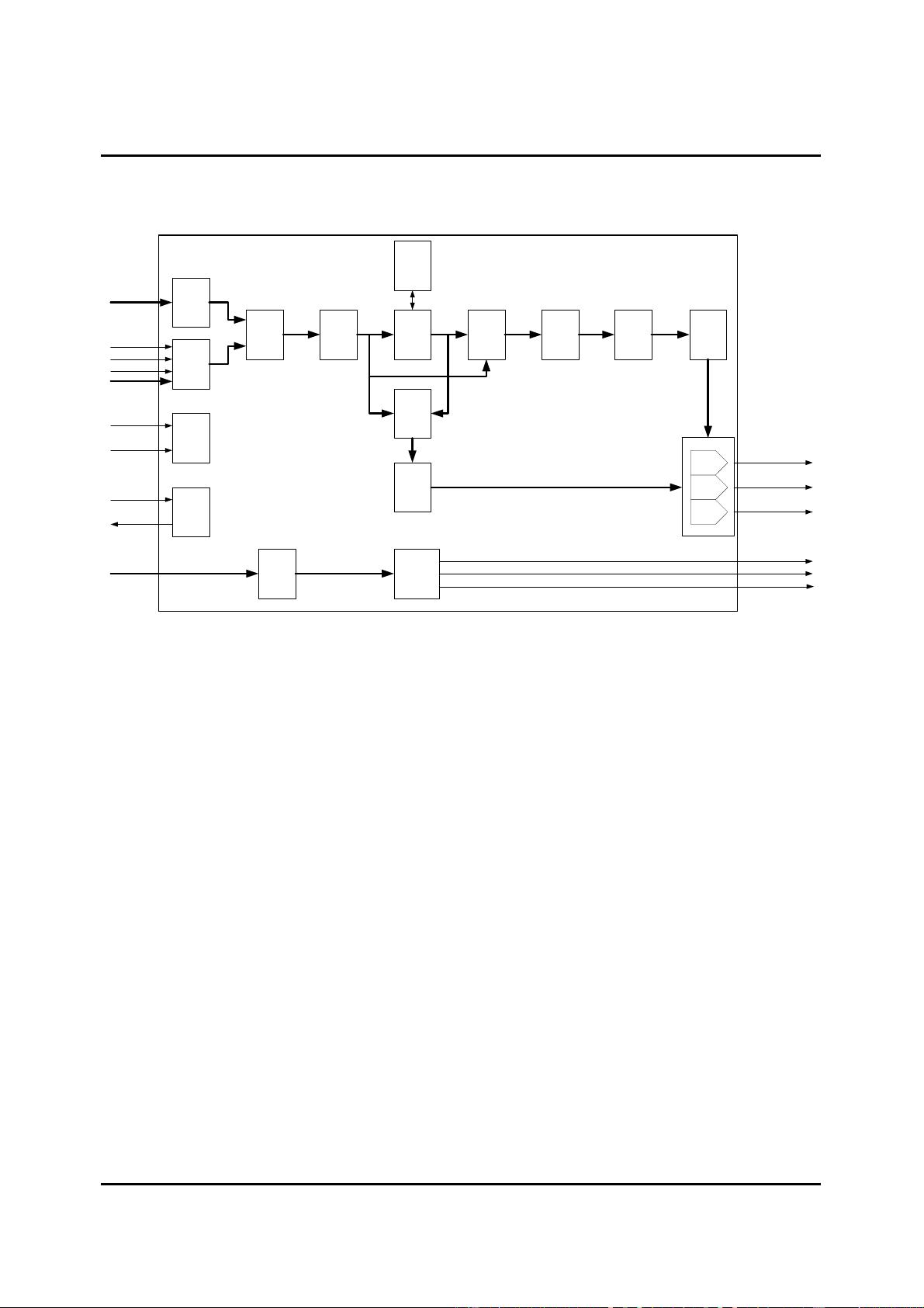
CH7025/CH7026 TV/VGA Encoder
FEATURES GENERAL DESCRIPTION
• Support multiple output formats. Such as SDTV format
(NTSC and PAL), HDTV format for 480p,576p,720p and
1080i, analog RGB output for VGA. Sync signals can be
provided in separated or composite manner
(Programmable composite sync generation).
• Three on-chip 10-bit high speed DACs providing flexible
output capabilities. Such as single, double or triple CVBS
outputs, YPbPr output, RGB output and simultaneous
CVBS and S-video outputs.
• Internal embedded 16Mbits SDRAM is used as frame
buffer. Supporting for frame rate conversion. 90/180/270
degree image rotation and vertical or horizontal flip
functions are supported.
• Programmable 24-bit/18-bit/16-bit/15-bit/12-bit/8-bit
digital input interface supports various RGB (RGB888,
RGB666, RGB565 and etc), YCbCr (4:4:4 YCbCr,
ITU656) and 2x or 3x multiplexed input. CPU/Memory
interface are supported.
• Support for flexible input resolution is up to 800x800 and
1024x680. 320x240, 640x480, 960x720 are support.
• Bypass mode is supported.
• Flexible up and down scaling engine is embedded
including de-flickering capability. Text enhancement is
supported.
• Pixel by pixel brightness, contrast, hue and saturation
adjustment for each kind of output are supported. For
RGB output, only brightness and contrast adjustment are
supported.
• Pixel by pixel horizontal position adjustment and line by
line vertical position adjustment are supported.
• Fully programmable through serial port. IO and SPC/SPD
voltage supported is from 1.2V to 3.3V.
• TV/Monitor connection detect capability.
• Programmable power management. DAC can be switched
off based on detection result (Driver support is required).
• Flexible pixel clock frequency from graphics controller is
supported (2.3MHz –120MHz). Flexible input clock from
crystal or oscillator is supported (2.3MHz – 64MHz).
• Macrovision
TM
7.1.L1 for SDTV is supported in CH7025
(CH7026 is Non-Macrovision part.). Macrovision
TM
copy
protection support for progressive scan TV (480p, 576p
CH7025 only).
• CGMS-A support for SDTV and HDTV (CH7025 only).
• Offered in BGA or QFP package.
The CH7025/CH7026 is a device targeting handheld
and similar consumer systems which accept digital
input signal. CH7025/CH7026 encodes and transmits
data through 10-bit DACs. The device is able to
encode the video signals and generate
synchronization signals SDTV format for NTSC and
PAL standards and HDTV format for
480p,576p,720p and 1080i. Analog RGB output and
composite SYNC signal are also supported. The
device accepts different data formats including RGB
and YCbCr (e.g. RGB565, RGB666, RGB888,
ITU656 like YCbCr, etc.).Both interlaced and non-
interlaced input data formats are supported. 16Mbit
SDRAM is embedded in package. Frame rate
conversion, Image rotation, zooming and scaling, are
supported.
Note: the above feature list is subject to change without notice. Please contact Chrontel for more information
and current updates.
CHRONTEL CH7025/CH7026
201-1000-001 Rev. 1.23, 03/31/2010
2
Input
data
format
decoder
RGB/YCbCr
CPU
interface
CSB
WEB
VSYNC
DIN
MUX
CSC
(YCbCr
to RGB)
Scaler
SDRAM
HUE
SAT
BRI
CON
VP
HP
TV
formater
MUX
BRI
CON
VP
HP
DAC 0
DAC 2
DAC 1
R/Y/CVBS/Y_Svideo
G/Pb/CVBS/C-Svideo
B/Pr/CVBS
Serial
port
SPC
SPD
PLL
XI
XO
SYNC
position
adjust
H,V,DE
Composite
sync
generation
CSYNC
VSYNC
HSYNC
CSC
(RGB to
YUV)
MUX
Figure 1: CH7025/CH7026 Block Diagram
CHRONTEL CH7025/CH7026
201-1000-001 Rev. 1.23, 03/31/2010 3
Table of Contents
FEATURES.................................................................................................................................................1
G
ENERAL DESCRIPTION ..........................................................................................................................1
1.0 PIN-OUT......................................................................................................................................6
1.1 Package Diagram .......................................................................................................................................6
1.2 Pin Description ..........................................................................................................................................7
2.0 FUNCTIONAL DESCRIPTION....................................................................................................11
2.1 Input Interface .......................................................................................................................................11
2.1.1 Overview..........................................................................................................................................11
2.1.2 Input Clock and Data Timing Diagram............................................................................................11
2.1.3 Input Data Voltage...........................................................................................................................12
2.1.4 Input Data Format............................................................................................................................12
2.2 Chip Output ...........................................................................................................................................14
2.2.1 TV Output........................................................................................................................................14
2.2.2 VGA Output.....................................................................................................................................15
2.2.3 Video DAC Output ..........................................................................................................................15
2.2.4 DAC Single/Double Termination ....................................................................................................15
2.2.5 Video DAC Connection Detect .......................................................................................................15
2.2.6 Picture Enhancement .......................................................................................................................15
2.2.7 Color Sub-carrier Generation...........................................................................................................15
2.2.8 ITU-R BT.470 Compliance .............................................................................................................16
2.3 Testing Functions and Power Down Mode..........................................................................................16
2.3.1 Test Pattern Select ...........................................................................................................................16
2.3.2 SDRAM Power Down .....................................................................................................................16
2.4 Serial Port...............................................................................................................................................16
2.4.1 Introduction......................................................................................................................................16
2.4.2 Electrical Characteristics of the Serial Port ........................................................................................17
2.4.3 Transfer Protocol ..............................................................................................................................17
2.4.4 Chrontel Encoder Write Cycle Protocol (R/W* = 0)..........................................................................18
2.4.5 Chrontel Encoder Read Cycle Protocol (R/W* = 1)...........................................................................19
3.0 REGISTER CONTROL ...............................................................................................................21
3.1 Control Registers Index ...........................................................................................................................21
3.2 Control Registers Map.............................................................................................................................24
3.3 Register Descriptions...............................................................................................................................27
4.0 ELECTRICAL SPECIFICATIONS ...............................................................................................55
4.1 Absolute Maximum Ratings ....................................................................................................................55
4.2 Recommended Operating Conditions ......................................................................................................55
4.3 Electrical Characteristics .........................................................................................................................56
4.4 Digital Inputs / Outputs............................................................................................................................56
4.5 AC Specifications ....................................................................................................................................57
5.0 PACKAGE DIMENSIONS ...........................................................................................................58
6.0 R
EVISION HISTORY .................................................................................................................60
CHRONTEL CH7025/CH7026
201-1000-001 Rev. 1.23, 03/31/2010
4
CHRONTEL CH7025/CH7026
201-1000-001 Rev. 1.23, 03/31/2010 5
FIGURES AND TABLES
List of Figures
Figure 1: CH7025/CH7026 Block Diagram ......................................................................................................2
Figure 2: BGA Package (Top View) .................................................................................................................6
Figure 3: 80 Pin LQFP Package ........................................................................................................................7
Figure 4: Clock and Data Input Timing in 3x Multiplexed Mode ..................................................................11
Figure 5: SDR and DDR Input Data Formats..................................................................................................11
Figure 6: Horizontal Input Timing...................................................................................................................12
Figure 7: Vertical Input Timing.......................................................................................................................12
Figure 8: CPU/MEMORY Interface Timing ...................................................................................................12
Figure 9: The Connection of the Serial Port Interface .....................................................................................17
Figure 10: Acknowledge Protocol ...................................................................................................................19
Figure 11:Single-step Write Cycles (2 cycles) ................................................................................................19
Figure 12: Auto-Increment Write Cycle..........................................................................................................19
Figure 13: Single-step Read Cycles (2 cycles) ................................................................................................20
Figure 14:Auto-increment Read Cycles...........................................................................................................20
Figure 15: 80 Pin TFBGA Package .................................................................................................................58
Figure 16: 80 Pin LQFP Package ....................................................................................................................59
List of Tables
Table 1: Pin Name Description (BGA Package) ...............................................................................................7
Table 2: Pin Name Descriptions (LQFP80 Package).........................................................................................9
Table 3: Input Data Format.............................................................................................................................13
Table 4: Supported SDTV Standards...............................................................................................................14
Table 5: Supported EDTV/HDTV Standards ..................................................................................................14
Table 6: Composite Sync Type........................................................................................................................15
Table 7: Video DAC Configurations for CH7025/CH7026 ............................................................................15
Table 8: Test Pattern Selection ........................................................................................................................16
Table 9: Control Registers Index.....................................................................................................................21
Table 10: Serial Port Register Map..................................................................................................................24
Table 11 : DAC Power Down Control Bits .....................................................................................................28
Table 12: Multiple TV Output Configuration..................................................................................................30
Table 13: DAC Output Swapping Sequence....................................................................................................30
Table 14 : HIGH,SWAP Format......................................................................................................................31
Table 15: SDTV/VGA Output Format ............................................................................................................31
Table 16: Macrovision Level Mode MVMODE[1:0]......................................................................................46
Table 17 : EDTV/HDTV Output Format.........................................................................................................48
Table 18: Attached Display Mapping ..............................................................................................................54
剩余60页未读,继续阅读
资源评论
- yangcenhao_1232012-09-11datasheet而已 我还以为是配置教程
- coolerchen10022013-01-06我也以为是配置教程~~~
- ijiancj2013-01-08比较全,有参考意义!
wdl1127
- 粉丝: 64
- 资源: 20
上传资源 快速赚钱
- 我的内容管理 展开
- 我的资源 快来上传第一个资源
- 我的收益 登录查看自己的收益
- 我的积分 登录查看自己的积分
- 我的C币 登录后查看C币余额
- 我的收藏
- 我的下载
- 下载帮助
安全验证
文档复制为VIP权益,开通VIP直接复制
信息提交成功