这是一款电源管理IC,芯片资料
需积分: 41 30 浏览量
2011-08-17
08:37:50
上传
评论 1
收藏 243KB PDF 举报


RT9045
1
RT9045-00P January 2009
www.richtek.com
Pin Configurations
Cost-Effective, 1.8A Sink/Source Bus Termination Regulator
Ordering Information
General Description
The RT9045 is a simple, cost-effective and high-speed
linear regulator designed to generate termination voltage
in double data rate (DDR) memory system to comply with
the devices requirements. The regulator is capable of
actively sinking or sourcing up to 1.8A while regulating an
output voltage to within 20mV. The output termination
voltage can be tightly regulated to track 1/2V
DDQ
by two
external voltage divider resistors or the desired output
voltage can be pro-grammed by externally forcing the
REFEN pin voltage.
The RT9045 also incorporates a high-speed differential
amplifier to provide ultra-fast response in line/load transient.
Other features include extremely low initial offset voltage,
excellent load regulation, current limiting in bi-directions
and on-chip thermal shut-down protection.
Features
zz
zz
z
Ideal for DDRII / DDRIII V
TT
Applications
zz
zz
z
Sink and Source Current :
1.8A Sink/Source @ V
IN
>>
>>
>
1.5V
1.0A Sink/Source @ V
IN
>>
>>
>
1V
zz
zz
z
Integrated Power MOSFETs
zz
zz
z
Generate Termination Voltage for DDR Memory
Interfaces
zz
zz
z
High Accuracy Output Voltage at Full-Load
zz
zz
z
Output Adjustment by Two External Resistors
zz
zz
z
Low External Component Count
zz
zz
z
Shutdown for Suspend to RAM (STR) Functionality
with High-Impedance Output
zz
zz
z
Current Limiting Protection
zz
zz
z
On-Chip Thermal Protection
zz
zz
z
RoHS Compliant
zz
zz
z
Stable with 2.2uF Output Ceramic Capacitor
Applications
z
Desktop PCs, Notebooks, and Workstations
z
Graphics Card Memory Termination
z
Set Top Boxes, Digital TVs, Printers
z
Embedded Systems
z
Active Termination Buses
z
DDR/II/III Memory Systems
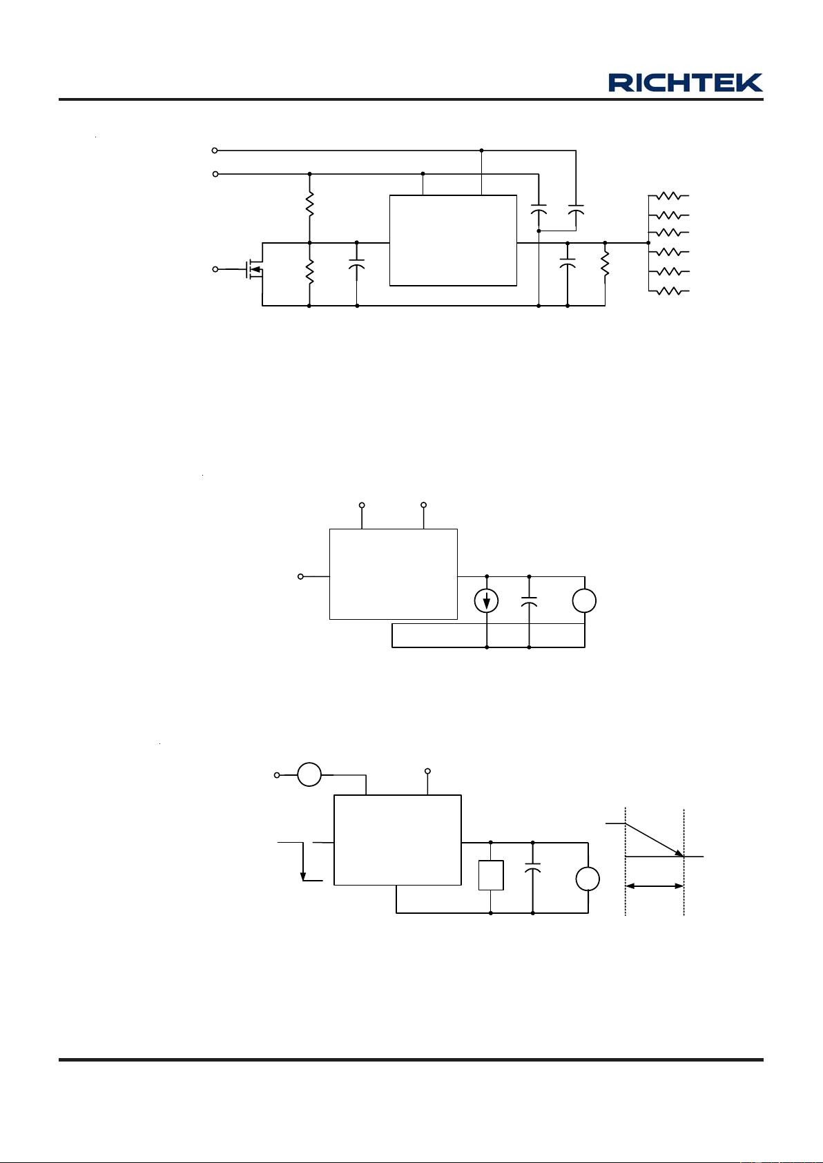
(TOP VIEW)
SOP-8 (Exposed Pad)
Note :
Richtek Green products are :
RoHS compliant and compatible with the current require-
ments of IPC/JEDEC J-STD-020.
Suitable for use in SnPb or Pb-free soldering processes.
100%matte tin (Sn) plating.
Package Type
SP : SOP-8 (Exposed Pad)
RT9045
Operating Temperature Range
G : Green (Halogen Free with Commer-
cial Standard)
VIN
GND
REFEN
VOUT
NC
NC
NC
VCNTL
GND
2
3
4
5
6
7
8
9
剩余11页未读,继续阅读
资源评论


