没有合适的资源?快使用搜索试试~ 我知道了~
AN0061 从MM32F0010移植到MM32F0020(英文版)
需积分: 5 0 下载量 194 浏览量
2024-03-06
09:08:14
上传
评论
收藏 599KB PDF 举报
温馨提示
试读
21页
AN0061 从MM32F0010移植到MM32F0020(英文版)
资源推荐
资源详情
资源评论
www.mm32mcu.com
1
Migrating from MM32F0010 to MM32F0020
Introduction
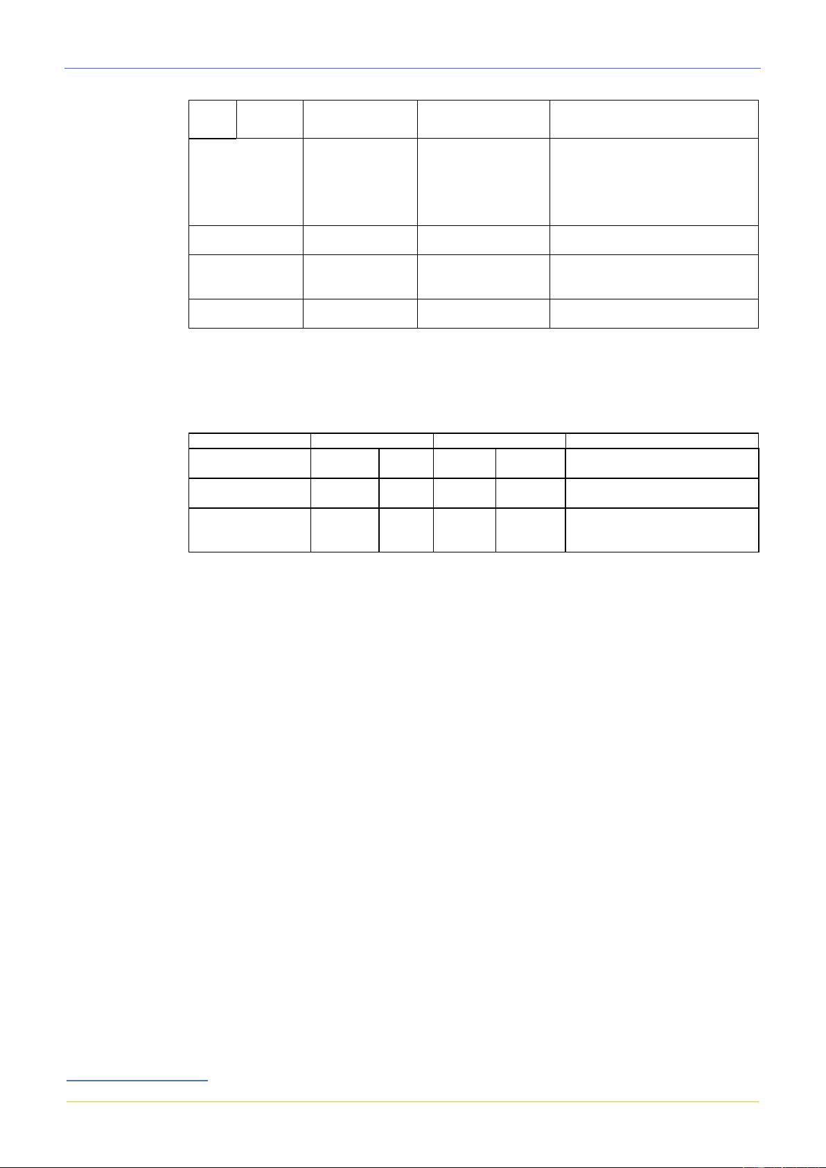
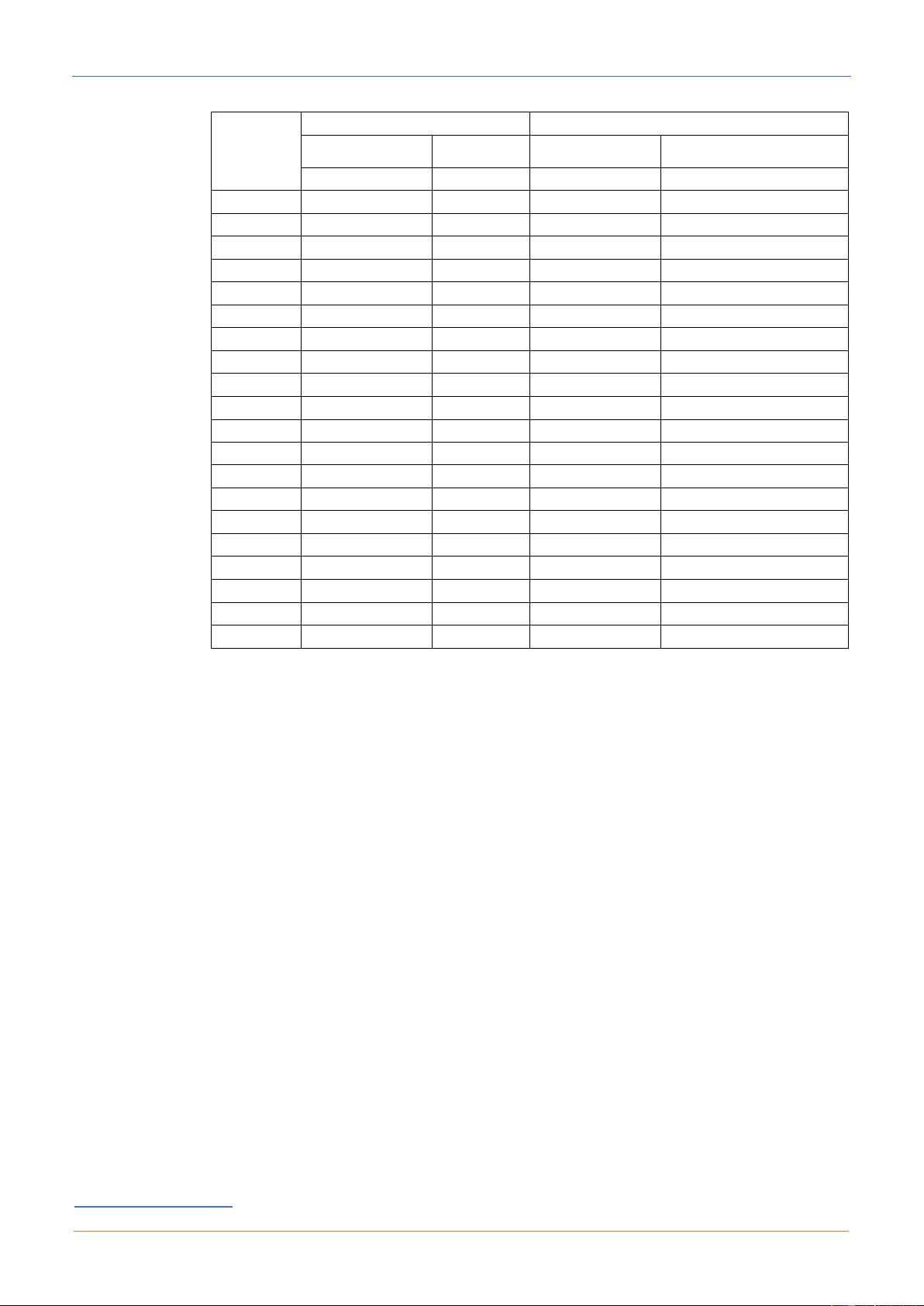
This application note describes and analyzes the differences between MM32F0010 and
MM32F0020, and provides steps required to migrate from the exsiting MM32F0010 device to
MM32F0020 device. Hardware difference, peripheral migration and firmware migration are
introduced respectively.
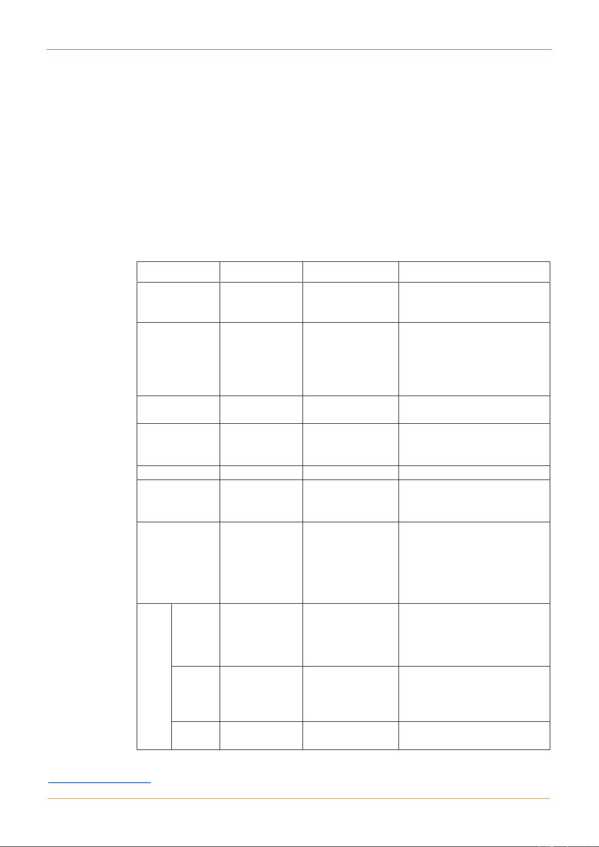
Table 1 Applicable series and models
Series
Models
MM32F0010
MM32F0010A1N
MM32F0010A1T
MM32F0020
MM32F0020B1N
MM32F0020B1T
AN0061
Application note
Rev 1.00 2021/12/16
AN0061 Migrating from MM32F0010 to MM32F0020
www.mm32mcu.com
2
1 Differences and similarities between
MM32F0020 and MM32F0010
1.1 Specification comparison of MM32F0020 and MM32F0010
MM32F0020 MCU are designed to be compatible with the features and
packages on MM32F0010. On the whole, MM32F0020 has richer functions
than MM32F0010.
Project
MM32F0010
MM32F0020
Descriptions
Core
Cortex-M0
Cortex-M0
Have the same core
FLASH
16 KB
32 KB
Flash start addresses, operation
controllers and read-protect setting
way are the same; since the Flash
Size of MM32F0020 is increased
to 32KB, the programming time is
also increased, while the Flash
Size of MM32F0010 is only 16KB.
SRAM
2 KB
2 KB
RAM start addresses and 2 KB
Size are the same.
Maximum CPU
frequency
48 MHz
48 MHz
MM2F0010 adopts the fixed
48MHz, while MM32F0020
supports PLL multiplier, with its
system clock up to 48 MHz.
Operating voltage
2.0V to 5.5V
2.0Vt o 5.5V
Same
GPIO
Not support
Tolerant
Not support Tolerant
GPIO characteristics are the
same. The functions of SWD pin
and the original package are
adjusted.
Boot
Not support ISP
support ISP and it
can be multiplexed to
more pins via
UART1 Boot.
MM32F0020 supports ISP function
and can be multiplexed to SWCLK
via BOOT0. UART1 supports
being multiplexed to more GPIOs.
Timer
Advance
d(4
channels
)
1
1
Support the output of 4 channels,
of which 3 channels support
complementary output and 1
channel supports single output.
Besides, MM32F0020’s TIM1 adds
PWM phase shift function.
General-
purpose
(3
channels
)
1
1
Same, both series have 16-bit
TIM3 and support the signle output
of 3 channels.
Basic
1
1
Same. They both support the
single output of 1 channel.
Migrating from MM32F0010 to MM32F0020 AN0061
www.mm32mcu.com
3
Systick
1
1
Same
ADC
1 x 12bit
1 x 12bit
Both support arbitrary sequence
channel conversion, while
MM32F0020 supports individual
configuration of each channel
sampling configuration, and
injected sampling.
UART
2
2
MM32F0020’s UART support IR
function
SPI
1
1
MM32F0010 only supports SPI,
while MM32F0020 supports SPI,
I2S and I/O Pad switch.
I2C
1
1
MM32F0020 also supports I/O Pad
switch.
1.2 Comparison of functional pins
MM32F0020 series MCU is compatible with GPIO pin and power supply pin of
MM32F0010 series.
MM32F0010
MM32F0020
Descriptions
Package
QFN20
TSSOP2
0
QFN20
TSSOP20
The supported package types are
the same.
Number of GPIO
18
18
18
18
MM32F0020 and MM32F0010
have the same GPIO number.
Boot0 Pin
Pin14
Pin17
MM32F0020 supports Boot0.
MM32F0010 does not support
Boot0.
Take the minimum system of TSSOP20 package chip as an example and the
comparison results are as follows:
AN0061 Migrating from MM32F0010 to MM32F0020
www.mm32mcu.com
4
TSSOP20
MM32F0010
MM32F0020
Pad Name
Alternate
Function
Pad Name
Alternate Function
GPIO/Power
AF0
GPIO/Power
AF0
1
PA11
PA11
2
PA12
PA12
3
PA3
PA3
4
PA14/NRST
SWDCLK
PA10/NRST
5
PB0/OSC_IN
PB0/OSC_IN
6
PB1/OSC_OUT
PB1/OSC_OUT
7
VSS
VSS
8
PA1
PA1
9
VDD
VDD
10
PA0
PA0
11
PA4
PA4
12
PA5
PA5
13
PA6
PA6
14
PA7
PA7
15
PA8
PA8
16
PA9
PA9
17
PA10
PA14/BOOT0
SWDCLK
18
PA13
SWDIO
PA13
SWDIO
19
PA15
PA15
20
PA2
PA2
Migrating from MM32F0010 to MM32F0020 AN0061
www.mm32mcu.com
5
Take the minimum system of QFN20 package chip as an example and the
comparison results are as follows:
QFN20
MM32F0010
MM32F0020
Pad Name
Alternate Function
Pad Name
Alternate
Function
GPIO
AF0
GPIO
AF0
1
PA14/NRST
SWDCLK
PA10/NRST
2
PB0/OSC_IN
PB0/OSC_IN
3
PB1/OSC_OUT
PB1/OSC_OUT
4
VSS
VSS
5
PA1
PA1
6
VDD
VDD
7
PA0
PA0
8
PA4
PA4
9
PA5
PA5
10
PA6
PA6
11
PA7
PA7
12
PA8
PA8
13
PA9
PA9
14
PA10
PA14/BOOT0
SWDCLK
15
PA13
SWDIO
PA13
SWDIO
16
PA15
PA15
17
PA2
PA2
18
PA11
PA11
19
PA12
PA12
20
PA3
PA3
Button
Pad
NC
NC
It can be seen from the above two tables that GPIO, power supply and reset
pin functions of MM32F0020 are basically compatible with power supply, reset
pin, WKUP PIN and GPIO functions of MM32F0010.
1. MM32F0020 is compatible with the power supply pins VDD/VSS of
MM32F0010.
2. Differences can be found in SWCLK in the multiplexed SWD interface.
3. After MM32F0010 is powered on, it has no Boot0 Pin function, while
MM32F0020 supports Boot0 Pin function and performs checkup at each
power-on. Thus, during power-on, for running on Main Flash if needed,
PA14/BOOTO Pin must be ensured as low level; for running on ISP if
needed, PA14/BOOT0 Pin must be ensured as high level.
4. Reset pin of MM32F0020 must keep high despite reset feature is enabled
or disabled.
剩余20页未读,继续阅读
资源评论
hepmp
- 粉丝: 1
- 资源: 58
上传资源 快速赚钱
- 我的内容管理 展开
- 我的资源 快来上传第一个资源
- 我的收益 登录查看自己的收益
- 我的积分 登录查看自己的积分
- 我的C币 登录后查看C币余额
- 我的收藏
- 我的下载
- 下载帮助
最新资源
- mysql查询语句汇总.zip
- typora-x64-v0.9.93,windows,64位,markdown工具,文本编辑器
- 基于C语言的neon_osd_Draw ARM Neon加速OSD点阵设计源码
- 目标检测-工地工人安全设备佩戴检测数据集-3500张图-+对应VOC-COCO-YOLO三种格式标签+数据集划分脚本+训练日志
- 运筹学运输问题综合实验的实验报告
- home - 副本.vue
- imageProcess.py
- typora-linux-v0.11.18-amd64,linux,64位,markdown工具,文本编辑器
- 基于Java的sky-take-out云霄外卖管理系统设计源码
- SAP-可用性检查应用测试.docx
资源上传下载、课程学习等过程中有任何疑问或建议,欢迎提出宝贵意见哦~我们会及时处理!
点击此处反馈
安全验证
文档复制为VIP权益,开通VIP直接复制
信息提交成功