没有合适的资源?快使用搜索试试~ 我知道了~
SPD DDR4的参数
4星 · 超过85%的资源 需积分: 24 79 下载量 64 浏览量
2017-10-21
23:31:39
上传
评论 3
收藏 290KB PDF 举报
温馨提示
试读
66页
DDR4颗粒使用的过程需要控制器在初始化的时候下发SPD的配置,根据实际的使用情况适当修改参数,文档中对每一个参数做了详细的解释,便于大家学习
资源推荐
资源详情
资源评论
Release 23A
JEDEC Standard No. 21-C
Page 4.1.2.12.2 – 1
Annex L: Serial Presence Detect (SPD) for DDR4 SDRAM Modules
DDR4 SPD Document Release 2
UDIMM Revision 1.0
RDIMM Revision 1.0
LRDIMM Revision 1.0
1.0 Introduction
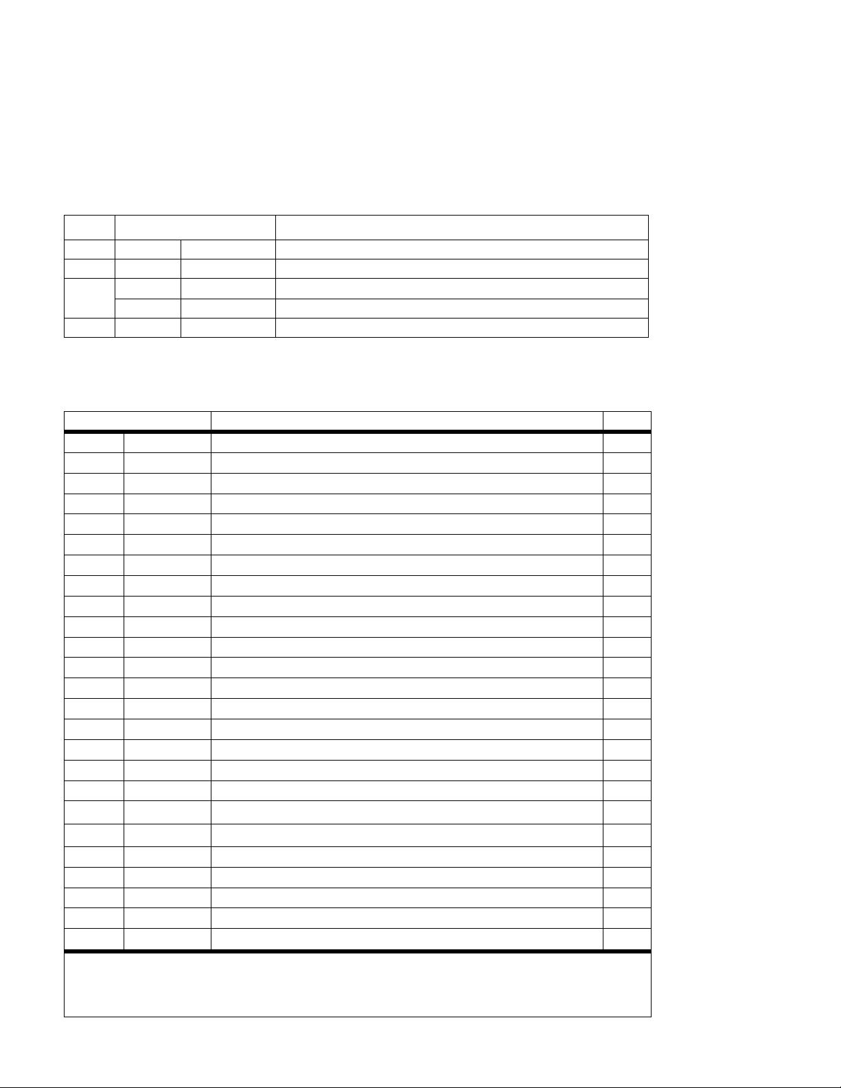
This annex describes the serial presence detect (SPD) values for all DDR4 modules. Differences between module types
are encapsulated in subsections of this annex. These presence detect values are those referenced in the SPD standard
document for ‘Specific Features’. The following SPD fields will be documented in the order presented in section 1.1 with
the exception of bytes 128~255 which are documented in separate annexes, one for each family of module types. Further
description of Byte 2 is found in Annex A of the SPD standard.
All unused entries will be coded as 0x00. All unused bits in defined bytes will be coded as 0 except where noted.
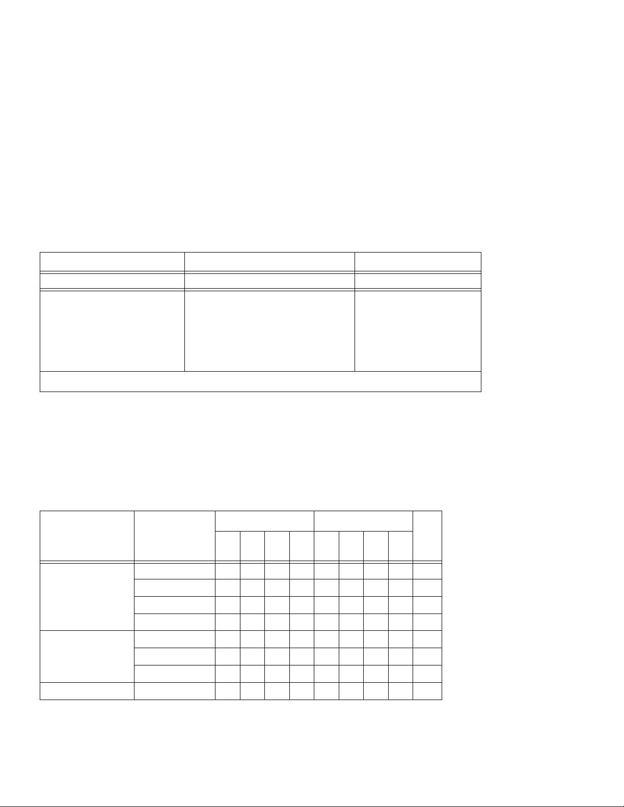
DDR4 generation systems are required to check the voltages supported by the DRAMs by reading the SPD and parsing
byte 6, the Module Nominal Voltage, before applying power to the DRAMs. All JEDEC standard modules allow applying
SPD power without applying a supply voltage to the DRAMs in order to support this requirement.
Timing parameters in the SPD represent the operation of the module including all DRAMs and support devices at the
lowest supported supply voltage (see SPD byte 11), and are valid from t
CKAVG
min to t
CKAVG
max (see SPD bytes 18 and
19).
To allow for maximum flexibility as devices evolve, SPD fields described in this document may support device
configuration and timing options that are not included in the JEDEC DDR4 SDRAM data sheet (JESD79-4). Please refer
to DRAM supplier data sheets or JESD79-4 to determine the compatibility of components.
Release 23A
JEDEC Standard No. 21-C
Page 4.1.2.12.2 – 2
1.1 Address map
The following is the SPD address map for all DDR4 modules. It describes where the individual lookup table entries will be
held in the serial EEPROM. Consistent with the definition of DDR4 generation SPD devices, which have four individual
write protection blocks of 128 bytes in length each, the SPD contents are aligned with these blocks as follows:
Block 0: Base Configuration and DRAM Parameters
The following table details the location of each byte in this block.
Block Range Description
0 0~127 0x000~0x07F Base Configuration and DRAM Parameters
1 128~255 0x080~0x0FF Module Specific Parameters -- See subsections L1, L2, and L3 for details
2
256~319 0x100~0x13F
Reserved -- must be coded as 0x00
320~383 0x140~0x17F Manufacturing Information
3 384~511 0x180~0x1FF End User Programmable
Byte Number
Function Described
Notes
0 0x000 Number of Serial PD Bytes Written / SPD Device Size / CRC Coverage 1, 2
1 0x001 SPD Revision
2 0x002 Key Byte / DRAM Device Type
3 0x003 Key Byte / Module Type
4 0x004 SDRAM Density and Banks 3
5 0x005 SDRAM Addressing 3
6 0x006 SDRAM Package Type 3
7 0x007 SDRAM Optional Features 3
8 0x008 SDRAM Thermal and Refresh Options 3
9 0x009 Other SDRAM Optional Features 3
10 0x00A Reserved -- must be coded as 0x00
11 0x00B Module Nominal Voltage, VDD 3
12 0x00C Module Organization
13 0x00D Module Memory Bus Width
14 0x00E Module Thermal Sensor
15 0x00F Extended module type
16 0x010 Reserved -- must be coded as 0x00
17 0x011 Timebases
18 0x012
SDRAM Minimum Cycle Time (t
CKAVG
min)
3
19 0x013
SDRAM Maximum Cycle Time (t
CKAVG
max)
3
20 0x014 CAS Latencies Supported, First Byte 3
21 0x015 CAS Latencies Supported, Second Byte 3
22 0x016 CAS Latencies Supported, Third Byte 3
23 0x017 CAS Latencies Supported, Fourth Byte 3
24 0x018
Minimum CAS Latency Time (t
AA
min)
3
Note 1 Number of SPD bytes written will typically be programmed as 384 bytes.
Note 2 Size of SPD device will typically be programmed as 512 bytes.
Note 3 From DDR4 SDRAM datasheet.
Note 4 These are optional, in accordance with the JEDEC specification.
Release 23A
JEDEC Standard No. 21-C
Page 4.1.2.12.2 – 3
Block 1: Module Specific Parameters
Bytes 128~255 (0x080~0x0FF) Parameters in this block are specific to the module type as selected by the contents of
SPD Key Byte 3. Refer to the appropriate annex for detailed byte descriptions.
25 0x019
Minimum RAS to CAS Delay Time (t
RCD
min)
3
26 0x01A
Minimum Row Precharge Delay Time (t
RP
min)
3
27 0x01B
Upper Nibbles for t
RAS
min and t
RC
min
3
28 0x01C
Minimum Active to Precharge Delay Time (t
RAS
min), Least Significant Byte
3
29 0x01D
Minimum Active to Active/Refresh Delay Time (t
RC
min), Least Significant Byte
3
30 0x01E
Minimum Refresh Recovery Delay Time (t
RFC1
min), LSB
3
31 0x01F
Minimum Refresh Recovery Delay Time (t
RFC1
min), MSB
3
32 0x020
Minimum Refresh Recovery Delay Time (t
RFC2
min), LSB
3
33 0x021
Minimum Refresh Recovery Delay Time (t
RFC2
min), MSB
3
34 0x022
Minimum Refresh Recovery Delay Time (t
RFC4
min), LSB
3
35 0x023
Minimum Refresh Recovery Delay Time (t
RFC4
min), MSB
3
36 0x024
Minimum Four Activate Window Time (t
FAW
min), Most Significant Nibble
3
37 0x025
Minimum Four Activate Window Time (t
FAW
min), Least Significant Byte
3
38 0x026
Minimum Activate to Activate Delay Time (t
RRD_S
min), different bank group
3
39 0x027
Minimum Activate to Activate Delay Time (t
RRD_L
min), same bank group
3
40 0x28
Minimum CAS to CAS Delay Time (t
CCD_L
min), same bank group
3
41~59 0x029~0x03B Reserved -- must be coded as 0x00
60~77 0x03C~0x04D Connector to SDRAM Bit Mapping
78~116 0x04E~0x074 Reserved -- must be coded as 0x00
117 0x75
Fine Offset for Minimum CAS to CAS Delay Time (t
CCD_L
min), same bank
group
118 0x76
Fine Offset for Minimum Activate to Activate Delay Time (t
RRD_L
min), same
bank group
3
119 0x77
Fine Offset for Minimum Activate to Activate Delay Time (t
RRD_S
min), different
bank group
3
120 0x078
Fine Offset for Minimum Activate to Activate/Refresh Delay Time (t
RC
min)
3
121 0x079
Fine Offset for Minimum Row Precharge Delay Time (t
RP
min)
3
122 0x07A
Fine Offset for Minimum RAS to CAS Delay Time (t
RCD
min)
3
123 0x07B
Fine Offset for Minimum CAS Latency Time (t
AA
min)
3
124 0x07C
Fine Offset for SDRAM Maximum Cycle Time (t
CKAVG
max)
3
125 0x07D
Fine Offset for SDRAM Minimum Cycle Time (t
CKAVG
min)
3
126 0x07E CRC for Base Configuration Section, Least Significant Byte
127 0x07F CRC for Base Configuration Section, Most Significant Byte
Byte Number
Function Described
Notes
Note 1 Number of SPD bytes written will typically be programmed as 384 bytes.
Note 2 Size of SPD device will typically be programmed as 512 bytes.
Note 3 From DDR4 SDRAM datasheet.
Note 4 These are optional, in accordance with the JEDEC specification.
Release 23A
JEDEC Standard No. 21-C
Page 4.1.2.12.2 – 4
Block 2, lower half: Reserved
Bytes 256~319 (0x100~0x13F) Reserved -- must be coded as 0x00.
Block 2, upper half: Manufacturing Information
Bytes 320~383 (0x140~0x17F) The following table details the location of each byte in this block.
Block 3: End User Programmable
Bytes 384~511 (0x180~0x1FF) Bytes in this block are reserved for use by end users.
Byte Number
Function Described
Notes
320 0x140 Module Manufacturer’s ID Code, Least Significant Byte
321 0x141 Module Manufacturer’s ID Code, Most Significant Byte
322 0x142 Module Manufacturing Location
323~324 0x143~0x144 Module Manufacturing Date
325~328 0x145~0x148 Module Serial Number
329~348 0x149~0x15C Module Part Number
349 0x15D Module Revision Code
350 0x15E DRAM Manufacturer’s ID Code, Least Significant Byte
351 0x15F DRAM Manufacturer’s ID Code, Most Significant Byte
352 0x160 DRAM Stepping
353~381 0x161~0x17D Module Manufacturer’s Specific Data
382~383 0x17E~0x17F Reserved; must be coded as 0x00
Release 23A
JEDEC Standard No. 21-C
Page 4.1.2.12.2 – 5
2.0 Details of each byte
2.1 General Configuration Section: Bytes 0~127 (0x000~0x07F)
This section contains defines parameters that are common to all DDR4 module types.
Byte 0 (0x000): Number of Bytes Used / Number of Bytes in SPD Device / CRC Coverage
The least significant nibble of this byte describes the total number of bytes used by the module manufacturer for the SPD
data and any (optional) specific supplier information. The byte count includes the fields for all required and optional data.
Bits 6~4 describe the total size of the serial memory used to hold the Serial Presence Detect data.
Byte 1 (0x001): SPD Revision
This byte describes the compatibility level of the encoding of the bytes contained in the SPD EEPROM, and the current
collection of valid defined bytes. Software should examine the upper nibble (Encoding Level) to determine if it can
correctly interpret the contents of the module SPD. The lower nibble (Additions Level) can optionally be used to
determine which additional bytes or attribute bits have been defined; however, since any undefined additional byte must
be encoded as 0x00 or undefined attribute bit must be defined as 0, software can safely detect additional bytes and use
safe defaults if a zero encoding is read for these bytes.
The Additions Level is never reduced even after an increment of the Encoding Level. For example, if the current SPD
revision level were 1.2 and a change in Encoding Level were approved, the next revision level would be 2.2. If additions
to revision 2.2 were approved, the next revision would be 2.3. Changes in the Encoding Level are extremely rare,
however, since they can create incompatibilities with older systems.
Bit 7 Bits 6~4 Bits 3~0
Reserved SPD Bytes Total SPD Bytes Used
Reserved Bit [6, 5, 4] :
000 = Undefined
001 = 256
010 = 512
All others reserved
Bit [3, 2, 1, 0] :
0000 = Undefined
0001 = 128
0010 = 256
0011 = 384
0100 = 512
All others reserved
Note 1 Typical programming of bits 3~0 will be 0011 (384 bytes).
Production Status SPD Revision
Encoding Level Additions Level
Hex
Bit
7
Bit
6
Bit
5
Bit
4
Bit
3
Bit
2
Bit
1
Bit
0
Pre-production
Revision 0.0 0000000000
Revision 0.1 0000000101
... ........ .
Revision 0.9 0000100109
Production
Revision 1.0 0001000010
Revision 1.1 0001000111
... ...........
Undefined Undefined 11111111FF
剩余65页未读,继续阅读
资源评论
- 尘风掠过2019-08-17还不错,支持作者!
fendouyefei
- 粉丝: 2
- 资源: 1
上传资源 快速赚钱
- 我的内容管理 展开
- 我的资源 快来上传第一个资源
- 我的收益 登录查看自己的收益
- 我的积分 登录查看自己的积分
- 我的C币 登录后查看C币余额
- 我的收藏
- 我的下载
- 下载帮助
安全验证
文档复制为VIP权益,开通VIP直接复制
信息提交成功