没有合适的资源?快使用搜索试试~ 我知道了~
资源推荐
资源详情
资源评论
Release 26
JEDEC Standard No. 21-C
Page 4.1.2.L-4 – 1
JESD 21-C Section Title: Annex L: Serial Presence Detect (SPD) for DDR4 SDRAM Modules
Committee Document Reference Title: DDR4 SPD Document Release 4
Device Type Identifier: UDIMM Revision 1.1
RDIMM Revision 1.2
LRDIMM Revision 1.2
NVDIMM-N Revision 1.1
1 Scope
This annex describes the serial presence detect (SPD) values for all DDR4 modules. The SPD data provides critical information about
all modules on the memory channel and is intended to be use by the system's BIOS in order to properly initialize and optimize the
system memory channels. The storage capacity of the SPD EEPROMs is limited, so a number of techniques are employed to optimize
the use of these bytes, including overlays and run length limited coding.
All unused entries will be coded as 0x00. All unused bits in defined bytes will be coded as 0 except where noted.
Timing parameters in the SPD represent the operation of the module including all DRAMs and support devices at the lowest
supported supply voltage (see SPD byte 11), and are valid from t
CKAVG
min to t
CKAVG
max (see SPD bytes 18 and 19).
To allow for maximum flexibility as devices evolve, SPD fields described in this document may support device configuration and
timing options that are not included in the JEDEC DDR4 SDRAM data sheet (JESD79-4). Please refer to DRAM supplier data sheets
or JESD79-4 to determine the compatibility of components.
2 History
Computer main memory buses have traditionally been defined by the generation of memory attached to the bus, e.g., EDO, SDRAM,
DDR1, etc. The bus interface protocol and characteristics have largely been defined by the memory type. Clock frequency, CAS
latencies, refresh recovery times and similar parameters defined the timing of signals between memory controller and the memory,
and parameters such as number of ranks installed and device widths allowed system software to determine the memory capacity and
similar high level characteristics of each module.
Over time, the memory bus has been extended to include additional features for application specific requirements. Registered
DIMMs, for example, increased total capacity by buffering the loading of the address bus signals, allowing more DRAM to be
installed. Similarly, Load Reduced DIMMs buffered the data bus as well, allowing even more ranks of memory to be supported. As
each new extension to the function of the memory bus was introduced, system software combined knowledge of those extensions
with information programmed into the EEPROM in the SPD to determine how to use and optimize the new features. Using the
RDIMM as an example, systems understood than an additional clock of latency needed to be added to the DRAM latency to
accommodate propagation delay through the register.
In later generations, the DRAM to host interface is completely virtualized. A memory module may have no DRAM at all, yet may use
the DRAM bus to communicate with the host by emulating the DRAM channel interface. These virtual interfaces must appear to the
system as one of the base module types, i.e., UDIMM, RDIMM, or LRDIMM. Modules that incorporate at least one non-DRAM
media type for the purpose of main memory data storage are called “hybrid”, they act like a DRAM but on the other side of the
interface protocol are some other memory type(s).
3 SPD Architecture
The SPD contents architecture must support the many variations of module types while remaining efficient. A system of overlay
information selected through the use of “key bytes”, or selectors for the type of information to load has been implemented. The
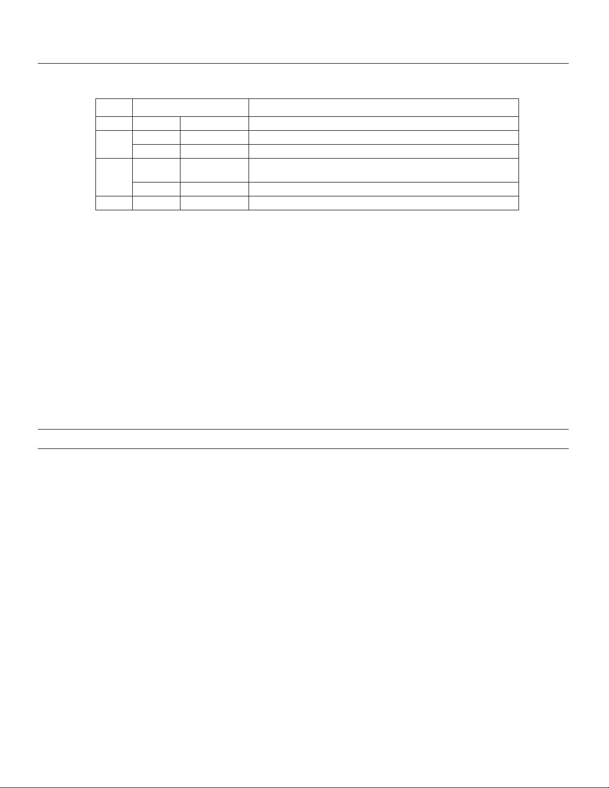
following DDR4 module SPD address map describes where the individual lookup table entries will be held in the serial EEPROM.
Consistent with the definition of DDR4 generation SPD devices (EE1004 and TSE2004) which have four individual write protection
blocks of 128 bytes in length each, the SPD contents are aligned with these blocks as shown in Table 1:
Release 26
JEDEC Standard No. 21-C
Page 4.1.2.L-4 – 2
Operating parameters for the different module types are defined in the following subsections and will reside in the appropriate
address ranges of the EEPROM address map depending on the module type. Please see Overlay Schema for further detail.
1. Section 9 - Standard Module Parameter - Overlay Bytes 128-191
• Section 9.1 - UDIMMs
• Section 9.2 - RDIMM
• Section 9.3 - LRDIMM
2. Section 10 - Hybrid Module Parameters - Overlay Bytes 192 - 255
• Section 10 .1 NVDIMM
3. Section 11 - Hybrid Module Extended Function Parameters - Overlay Bytes 256-319
• Section 11.1 - Energy Backed Byte Addressable NVDIMM
• Section 11.2 - Energy Backed Block Addressable NVDIMM
• Section 11.3 - Non-Energy Backed Byte Addressable NVDIMM
4 Overlay Schema
The following Schema exemplify the manner in which the base configuration information along with the appropriate subsections are
to be overlaid onto the appropriate address spaces in order to provide a complete definition of the module.
4.1 UDIMM Overlay Schema
Table 2 shows the UDIMM overlay schema.
Key Byte 2 contains value 0x0C or 0x0E
Key Byte 3 contains any of the following values:
• 0x02, UDIMM
• 0x03, SO-DIMM
• 0x06, Mini-UDIMM
• 0x09, 72b-SO-UDIMM
• 0x0C, 16b-SO-DIMM
• 0x0D, 32b-SO-DIMM
Table 1 — SPD Contents Architecture
Block Range Description
0 0~127 0x000~0x07F Base Configuration and DRAM Parameters
1
128~191 0x080~0x0BF Standard Module Parameters -- See annexes L.1.x for details
192~255 0x0C0~0x0FF Hybrid Module Parameters -- See annexes L.2.x for details
2
256~319 0x100~0x13F
Hybrid Module Extended Function Parameters - See Annexes L.3.x for
details
320~383 0x140~0x17F Manufacturing Information
3 384~511 0x180~0x1FF End User Programmable
3 SPD Architecture (Cont’d)
Release 26
JEDEC Standard No. 21-C
Page 4.1.2.L-4 – 3
4.2 RDIMM Overlay Schema
Table 3 shows the RDIMM overlay schema.
Key Byte 2 contains value 0x0C or 0x0E
Key Byte 3 contains any of the following values:
• 0x01, RDIMM
• 0x05, Mini-RDIMM
• 0x08, 72b-SO-RDIMM
4.3 LRDIMM Overlay Schema
Table 4 shows the LRDIMM overlay schema.
Key Byte 2 contains value 0x0C or 0x0E
Key Byte 3 contains any of the following values:
• 0x04, LRDIMM
Table 2 — UDIMM Overlay Schema
Block Range Description
0 0~127 Base Configuration and DRAM Parameters
1
128~191 Insert Section 9.1: Unbuffered Memory Module Types
192~255 Unused
2
256~319
Reserved
320~383 Module Supplier’s Data
3 384~511 End User Programmable
Table 3 — RDIMM Overlay Schema
Block Range Description
0 0~127 Base Configuration and DRAM Parameters
1
128~191 Insert Section 9.2: RDIMM Memory Module Types
192~255 Unused
2
256~319
Reserved
320~383 Module Supplier’s Data
3 384~511 End User Programmable
Table 4 — LRDIMM Overlay Schema
Block Range Description
0 0~127 Base Configuration and DRAM Parameters
1
128~191 Insert Section 9.3: LRDIMM Memory Module Types
192~255 Unused
2
256~319
Reserved
320~383 Module Supplier’s Data
3 384~511 End User Programmable
4 Overlay Schema (Cont’d)
4.1 UDIMM Overlay Schema (Cont’d)
Release 26
JEDEC Standard No. 21-C
Page 4.1.2.L-4 – 4
4.4 Hybrid DIMM Overlay Schema
Table 5 shows the Hybrid DIMM overlay schema.
Key Byte 2 contains value 0x0C or 0x0E
Key Byte 3 contains any of the following values:
• 0x9M, NVDIMM - Non-volatile DIMM; M defines base architecture
After programming the SPD contents, suppliers of JEDEC compliant modules must set the write protect bits for SPD device blocks 0
and 1 and must not set the write protect bit for block 3. Write protection of block 2 is required for modules using the Extended
Function Parameter Block, such as NVDIMMs. See the EE1004-v/TSE2004av Device Specification for details on the SWPn
command protocol.
5 Parsing the SPD
Table 6 provides relevant SPD bytes for parsing.
The system BIOS will acquire information from the SPD in order to properly configure the systems memory controller. It is assumed
the BIOS will parse the SPD data in the order listed below.
Step 1: Parse Byte 2 - Verify the installed DRAM type is supported.
The first step in parsing the SPD is to verify that the DRAM type installed is supported by looking at DRAM device type byte 2.
While it is usually not possible to physically plug in the wrong memory type, for example a DDR3 module size or key location should
prevent insertion into a DDR4 system, there are cases where byte 2 is used to prevent accidental use of an incompatible memory type
such as DDR4E modules in a DDR4-only system.
Table 5 — Hybrid DIMM Overlay Schema
Block Range Description
0 0~127 Base Configuration and DRAM Parameters
1
128~191 Insert Base Module Type Section 9.x
192~255 Insert Hybrid Memory Parameter Section 9.x
2
256~319
Insert Extended Function Parameter Block Section 9.x
320~383 Module Supplier’s Data
3 384~511 End User Programmable
Table 6 — Some Relevant SPD Bytes for Parsing
SPD Byte(s) Definition
1 SPD revision for this memory module
2 DRAM interface type presented or emulated
3 Memory module interface type
0~127 Base configuration and DRAM parameters
128~191 Module specific parameters
192~255 Hybrid memory parameters
204~219 NVDIMM function interface descriptors
256~319 Extended function parameter block
4 Overlay Schema (Cont’d)
Release 26
JEDEC Standard No. 21-C
Page 4.1.2.L-4 – 5
Step 2: Parse Byte 1 - Verify SPD compatibility. See Section 6 - SPD Revision Progression
The SPD revision byte 1 “encoding” nibble may be used to force legacy systems to reject newer modules. This would typically only
occur if a critical error were found in SPD encoding that would require a “fix”. In this case, as in the case of an unsupported DRAM
type, system initialization must be halted immediately.
The SPD revision stored in Byte 1 applies to all information for the module, including base information, module specific information,
and hybrid information. Each SPD revision exactly defines how many bytes are valid in all other SPD blocks. The number of
supported bytes (or bits) may increase from one SPD revision to another within each block as indicated by the “additions” nibble of
the SPD revision. For example, an SPD revision 1.3 has more bytes or bits defined than SPD revision 1.2.
This progression of SPD contents is important for the BIOS to DIMM compatibility model. An older system may have a BIOS that
only understands SPD revision 1.2 encoding, so if a module is installed that contains revision 1.3 information, the system can
accurately interpret all of the historical revision 1.2 information retained in the module that is the subset of the revision 1.3
specification. Similarly, if a module with SPD revision 1.1 information is installed, that same BIOS can interpret all information that
was current at the time that SPD 1.1 was defined. Therefore, BIOSes must maintain a knowledge of the active information for each
historical SPD revision in order to support older modules.
Step 3: Parse Byte 3 - Determine module type and appropriate overlays.
Key byte 3 for module type determines the subsequent use of overlay information. Byte 3 bits 3~0 define the host to module interface
style: unbuffered, registered, or load reduced. Standard module types are defined in Annexes L.1.x.
Key byte 3 also determines the presence of hybrid module types. Byte 3, bit 7 asserts if the module is hybrid, and Byte 3, bits 6~4
define the type of hybrid module. A hybrid module may appear to the system as a superset of any of the base module types. For
example, an NVDIMM may present a UDIMM, RDIMM, or LRDIMM compatible interface to the system. Because of this unique
second overlay for hybrid information on top of the base module type, the SPD revision for Hybrid modules must include all relevant
information for any of the base module types if applicable. Refer to SPD revision progression in Section 6 for more information.
If Byte 3, bits 7~4 indicate the presence of a Hybrid module type, the BIOS must parse two more overlays. Annex L.2, Hybrid
Module Parameters (Bytes 192~255) and Section 11 Hybrid Modules Extended Function Parameters (Bytes 256~319). As with the
module specific parameters, both of the Hybrid Module parameter sets may increase from SPD revision to revision.
Step 4: Parse Bytes 0-127 - Make base configuration settings to memory interface based on these bytes.
All module types are required to read and interpret this block of data to set up the DRAM type, maximum operating frequency, the
number of row, column, bank bits, write recovery time, etc. While these bytes primarily describe the timing of the DRAMs, timing
represents the capabilities of the module and it may be necessary to downgrade the timing based on other factors including layout or
support components on the module, such as registers.
Step 5: Parse Bytes 128-191 - Configure Standard module memory interface.
These bytes will be referenced and used by the system as needed based on the Standard module type that was determined after Byte 3
was parsed as indicated in Step 2. Bytes 128~191 are coded differently for each standard module type as defined in Section 9.
Step 6: Parse Bytes 192-255 (If Hybrid) - Read Hybrid Module parameters settings.
These bytes will be referenced and used by the system as needed based on the Hybrid module type that was determined after Byte 3
was parsed as indicated in Step 2. Function Format Interface Descriptors defined in bytes 204~205 through 218~219 will be read and
utilized as indicated in Step 7. Bytes 192~255 are coded differently for each Hybrid module type and defined in Section 10.
Step 7: Parse Bytes 256-319 (If Hybrid Extended Functions are specified).
These bytes will be referenced and used by the system as needed based on the Function Format interface descriptors read previously
during Step 6 from SPD bytes 204~205 through 218~219. Support up to 8 functions per Hybrid module can be defined within Bytes
256~319 and are coded based on Section 11.
For NVDIMM hybrid modules, parsing the two data blocks of hybrid memory parameters in SPD bytes 192~255 and the extended
function parameters in SPD bytes 256~319 is intimately related. Each function descriptor contains a 4-bit field in bits 13~10 that
creates an address pointer into the extended function parameter block. The formula is: 256 + 4 * function descriptor bits 13~10.
The extended function parameter blocks are run length limited, meaning that when one function parameter set stops the next set starts
5 Parsing the SPD (Cont’d)
剩余85页未读,继续阅读
资源评论
- A仁爱A2020-07-13非常好,值得学习
- jimmyzeng_cn2019-09-10非常好!!!!!!!!!!!!
- cquhuqx2019-05-20好,正着急想学学
中国永
- 粉丝: 4
- 资源: 11
上传资源 快速赚钱
- 我的内容管理 展开
- 我的资源 快来上传第一个资源
- 我的收益 登录查看自己的收益
- 我的积分 登录查看自己的积分
- 我的C币 登录后查看C币余额
- 我的收藏
- 我的下载
- 下载帮助
安全验证
文档复制为VIP权益,开通VIP直接复制
信息提交成功