AT89C52的使用手册

1
Features
• Compatible with MCS-51
™
Products
• 8K Bytes of In-System Reprogrammable Flash Memory
• Endurance: 1,000 Write/Erase Cycles
• Fully Static Operation: 0 Hz to 24 MHz
• Three-level Program Memory Lock
• 256 x 8-bit Internal RAM
• 32 Programmable I/O Lines
• Three 16-bit Timer/Counters
• Eight Interrupt Sources
• Programmable Serial Channel
• Low-power Idle and Power-down Modes
Description
The AT89C52 is a low-power, high-performance CMOS 8-bit microcomputer with 8K
bytes of Flash programmable and erasable read only memory (PEROM). The device
is manufactured using Atmel’s high-density nonvolatile memory technology and is
compatible with the industry-standard 80C51 and 80C52 instruction set and pinout.
The on-chip Flash allows the program memory to be reprogrammed in-system or by a
conventional nonvolatile memory programmer. By combining a versatile 8-bit CPU
with Flash on a monolithic chip, the Atmel AT89C52 is a powerful microcomputer
which provides a highly-flexible and cost-effective solution to many embedded control
applications.
8-bit
Microcontroller
with 8K Bytes
Flash
AT89C52
Not Recommended
for New Designs.
Use AT89S52.
Rev. 0313H–02/00
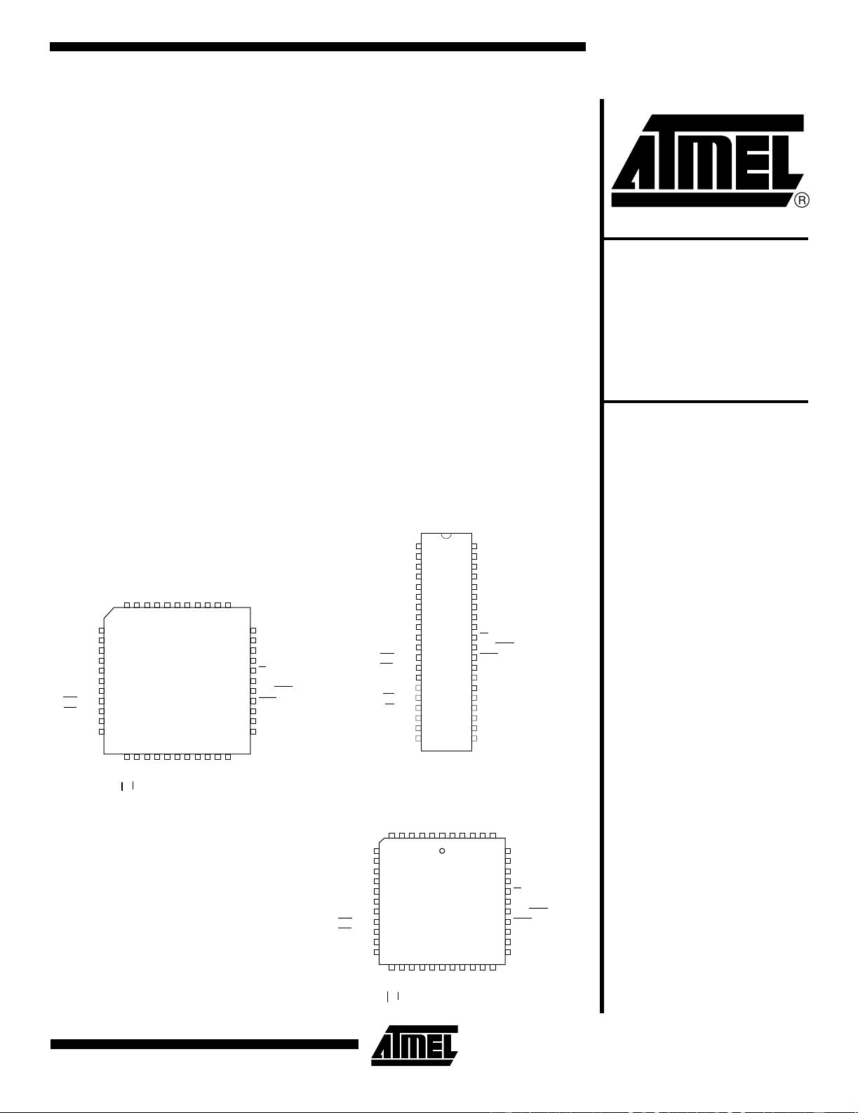
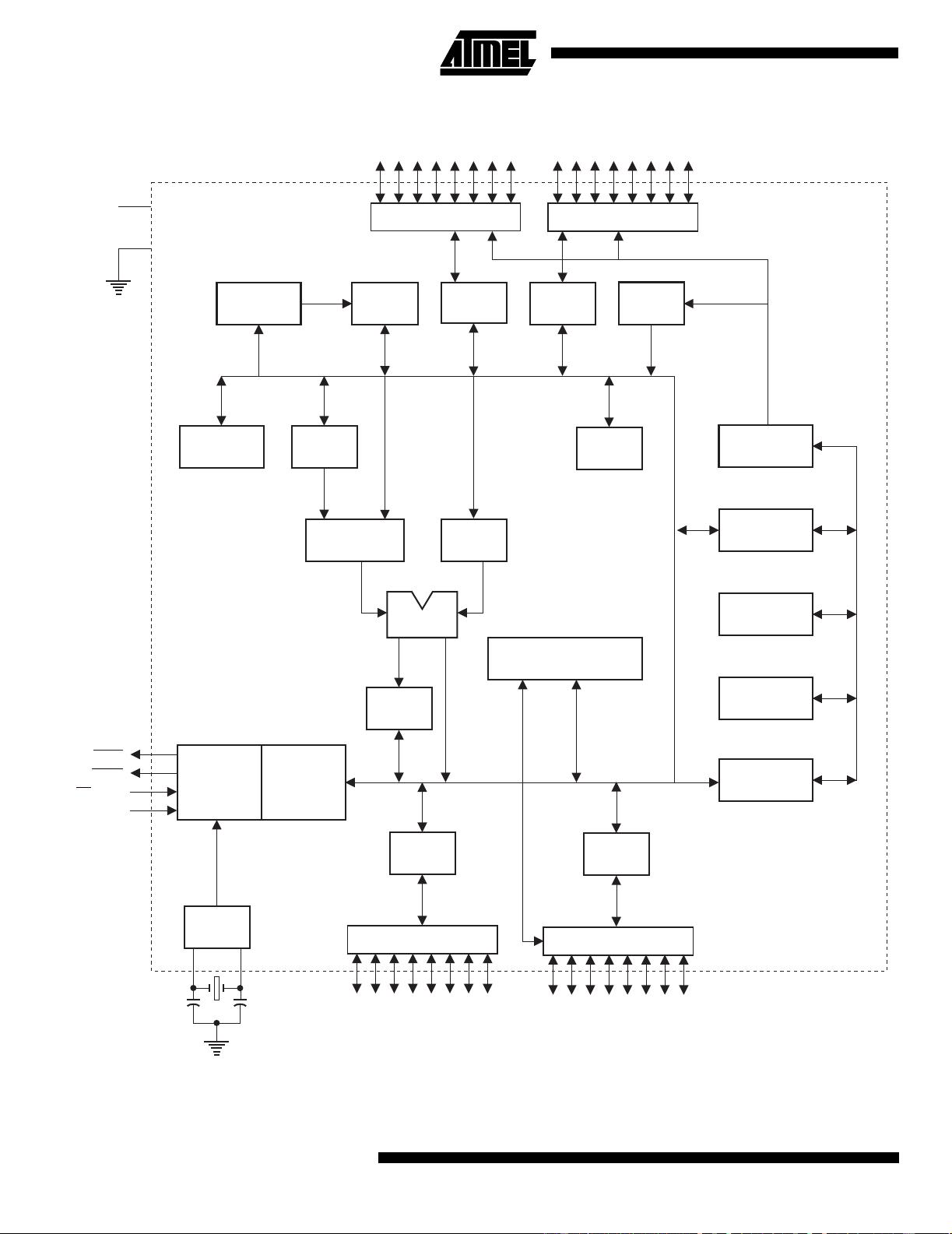
Pin Configurations
PQFP/TQFP
1
2
3
4
5
6
7
8
9
10
11
33
32
31
30
29
28
27
26
25
24
23
P1.5
P1.6
P1.7
RST
(RXD) P3.0
NC
(TXD) P3.1
(INT0) P3.2
(INT1) P3.3
(T0) P3.4
iT1) P3.5
P0.4 (AD4)
P0.5 (AD5)
P0.6 (AD6)
P0.7 (AD7)
EA/VPP
NC
ALE/PROG
PSEN
P2.7 (A15)
P2.6 (A14)
P2.5 (A13)
44
43
42
41
40
39
38
37
36
35
34
12
13
14
15
16
17
18
19
20
21
22
(WR) P3.6
(RD) P3.7
XTAL2
XTAL1
GND
NC
(A8) P2.0
(A9) P2.1
(A10) P2.2
(A11) P2.3
(A12) P2.4
P1.4
P1.3
P1.2
P1.1 (T2 EX)
P1.0 (T2)
NC
VCC
P0.0 (AD0)
P0.1 (AD1)
P0.2 (AD2)
P0.3 (AD3)
PDIP
1
2
3
4
5
6
7
8
9
10
11
12
13
14
15
16
17
18
19
20
40
39
38
37
36
35
34
33
32
31
30
29
28
27
26
25
24
23
22
21
(T2) P1.0
(T2 EX) P1.1
P1.2
P1.3
P1.4
P1.5
P1.6
P1.7
RST
(RXD) P3.0
(TXD) P3.1
(INT0) P3.2
(INT1) P3.3
(T0) P3.4
(T1) P3.5
(WR) P3.6
(RD) P3.7
XTAL2
XTAL1
GND
VCC
P0.0 (AD0)
P0.1 (AD1)
P0.2 (AD2)
P0.3 (AD3)
P0.4 (AD4)
P0.5 (AD5)
P0.6 (AD6)
P0.7 (AD7)
EA/VPP
ALE/PROG
PSEN
P2.7 (A15)
P2.6 (A14)
P2.5 (A13)
P2.4 (A12)
P2.3 (A11)
P2.2 (A10)
P2.1 (A9)
P2.0 (A8)
PLCC
7
8
9
10
11
12
13
14
15
16
17
39
38
37
36
35
34
33
32
31
30
29
P1.5
P1.6
P1.7
RST
(RXD) P3.0
NC
(TXD) P3.1
(INT0) P3.2
(INT1) P3.3
(T0) P3.4
(T1) P3.5
P0.4 (AD4)
P0.5 (AD5)
P0.6 (AD6)
P0.7 (AD7)
EA/VPP
NC
ALE/PROG
PSEN
P2.7 (A15)
P2.6 (A14)
P2.5 (A13)
6
5
4
3
2
1
44
43
42
41
40
18
19
20
21
22
23
24
25
26
27
28
(WR) P3.6
(RD) P3.7
XTAL 2
XTAL1
GND
NC
(A8) P2.0
(A9) P2.1
(A10) P2.2
(A11) P2.3
(A12) P2.4
P1.4
P1.3
P1.2
P1.1 (T2 EX)
P1.0 (T2)
NC
VCC
P0.0 (AD0)
P0.1 (AD1)
P0.2 (AD2)
P0.3 (AD3)
剩余23页未读,继续阅读
资源评论

 9034278872015-05-02很经典的资料,谢谢楼主分享
 stanly002015-09-20不错的单片机手册


