没有合适的资源?快使用搜索试试~ 我知道了~
flash手册(芯片管脚图)
5星 · 超过95%的资源 需积分: 31 41 下载量 91 浏览量
2010-08-27
16:51:33
上传
评论 4
收藏 771KB PDF 举报
温馨提示
试读
45页
flash手册(芯片管脚图),xiwang you suo bangzhu
资源推荐
资源详情
资源评论
FLASH MEMORY
1
K9F1208D0B
K9F1208U0B
K9F1208Q0B
Advance
Document Title
64M x 8 Bit NAND Flash Memory
Revision History
The attached datasheets are prepared and approved by SAMSUNG Electronics. SAMSUNG Electronics CO., LTD. reserve the right
to change the specifications. SAMSUNG Electronics will evaluate and reply to your requests and questions about device. If you have
any questions, please contact the SAMSUNG branch office near you.
Revision No.
0.0
Remark
Advance
History
Initial issue.
Draft Date
Apr. 24th 2004
Note : For more detailed features and specifications including FAQ, please refer to Samsung’s Flash web site.
http://www.samsung.com/Products/Semiconductor/Flash/TechnicalInfo/datasheets.htm
FLASH MEMORY
2
K9F1208D0B
K9F1208U0B
K9F1208Q0B
Advance
GENERAL DESCRIPTION
FEATURES
• Voltage Supply
- 1.8V device(K9F1208Q0B) : 1.70~1.95V
- 2.65V device(K9F1208D0B) : 2.4~2.9V
- 3.3V device(K9F1208U0B) : 2.7 ~ 3.6 V
• Organization
- Memory Cell Array : (64M + 2048K)bit x 8 bit
- Data Register : (512 + 16)bit x 8bit
• Automatic Program and Erase
- Page Program : (512 + 16)Byte
- Block Erase : (16K + 512)Byte
• Page Read Operation
- Page Size : (512 + 16)Byte
- Random Access : 15µs(Max.)
- Serial Page Access : 50ns(Min.)
64M x 8 Bit NAND Flash Memory
• Fast Write Cycle Time
- Program time : 200µs(Typ.)
- Block Erase Time : 2ms(Typ.)
• Command/Address/Data Multiplexed I/O Port
• Hardware Data Protection
- Program/Erase Lockout During Power Transitions
• Reliable CMOS Floating-Gate Technology
- Endurance : 100K Program/Erase Cycles
- Data Retention : 10 Years
• Command Register Operation
• Intelligent Copy-Back
• Unique ID for Copyright Protection
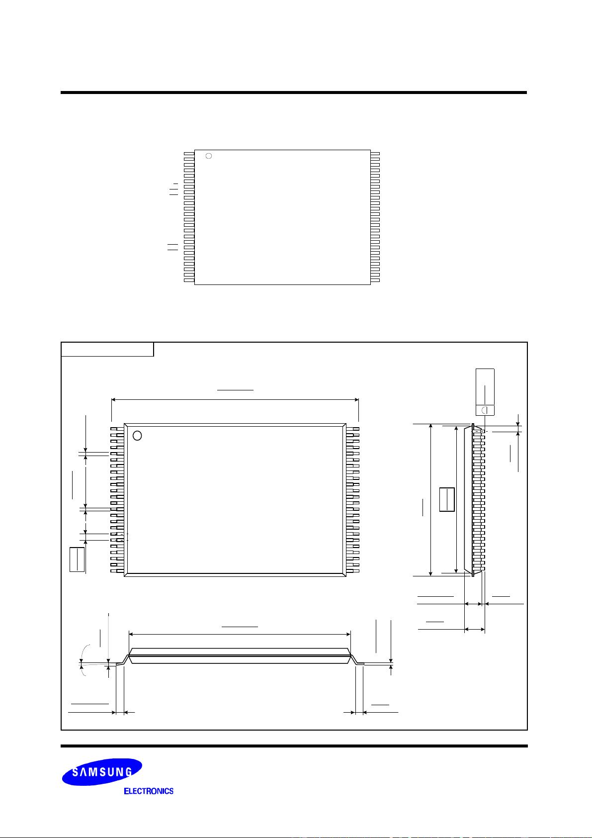
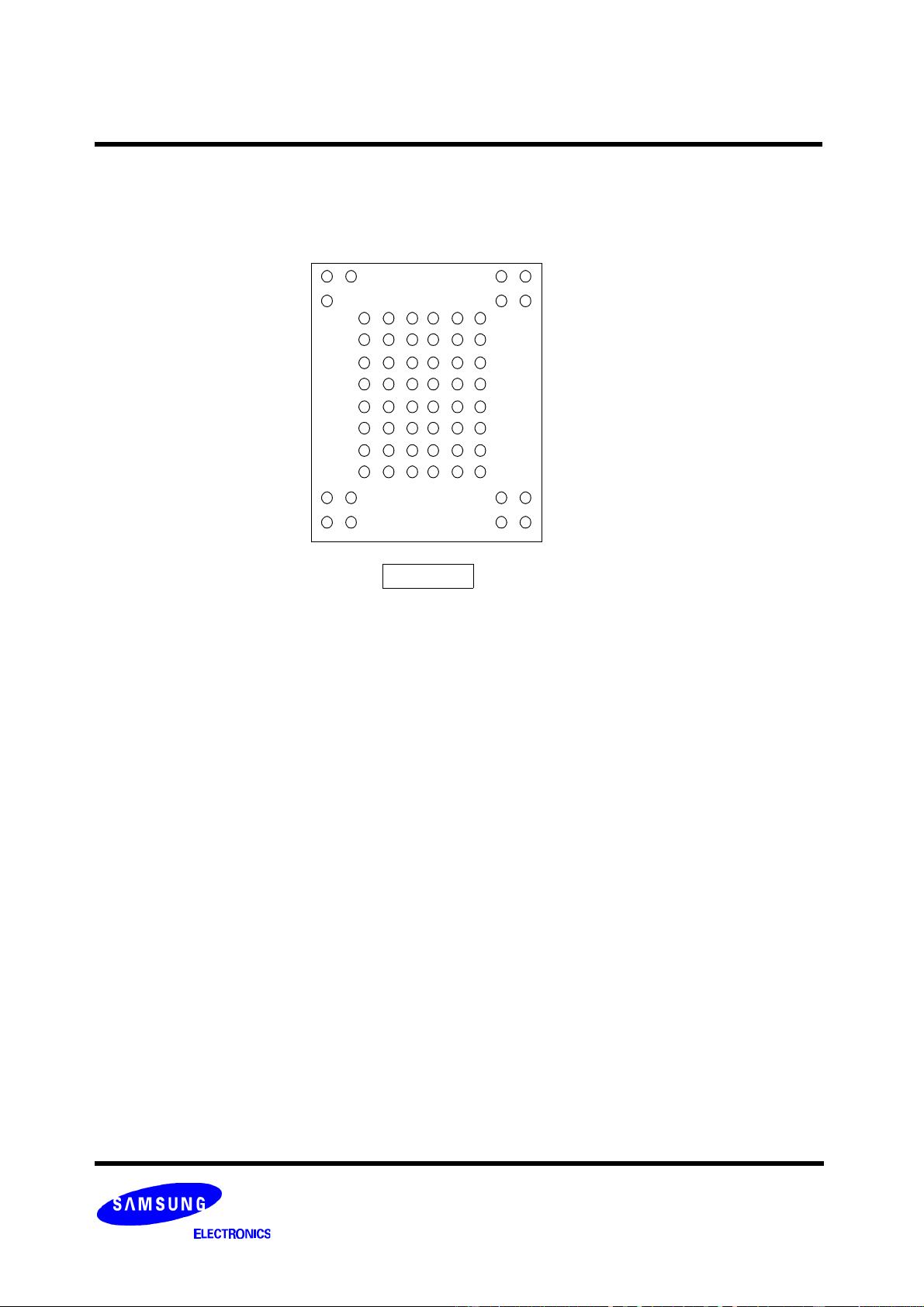
• Package
- K9F1208X0B-YCB0/YIB0
48 - Pin TSOP I (12 x 20 / 0.5 mm pitch)
- K9F1208X0B-GCB0/GIB0
63- Ball FBGA (8.5 x 13 , 1.0 mm width)
- K9F1208U0B-VCB0/VIB0
48 - Pin WSOP I (12X17X0.7mm)
- K9F1208X0B-PCB0/PIB0
48 - Pin TSOP I (12 x 20 / 0.5 mm pitch)- Pb-free Package
- K9F1208X0B-JCB0/JIB0
63- Ball FBGA - Pb-free Package
- K9F1208U0B-FCB0/FIB0
48 - Pin WSOP I (12X17X0.7mm)- Pb-free Package
* K9F1208U0B-V,F(WSOPI ) is the same device as
K9F1208U0B-Y,P(TSOP1) except package type.
Offered in 64Mx8bit the K9F1208X0B is 512M bit with spare 16M bit capacity. The device is offered in 1.8V, 2.65V, 3.3V Vcc. Its
NAND cell provides the most cost-effective solutIon for the solid state mass storage market. A program operation can be performed
in typical 200µs on the 528-byte page and an erase operation can be performed in typical 2ms on a 16K-byte block. Data in the page
can be read out at 50ns cycle time per byte. The I/O pins serve as the ports for address and data input/output as well as command
input. The on-chip write control automates all program and erase functions including pulse repetition, where required, and internal
verification and margining of data. Even the write-intensive systems can take advantage of the K9F1208X0B′s extended reliability of
100K program/erase cycles by providing ECC(Error Correcting Code) with real time mapping-out algorithm. The K9F1208X0B is an
optimum solution for large nonvolatile storage applications such as solid state file storage and other portable applications requiring
non-volatility.
PRODUCT LIST
Part Number Vcc Range PKG Type
K9F1208Q0B-D,H 1.70 ~ 1.95V FBGA
K9F1208D0B-Y,P
2.4 ~ 2.9V
TSOP1
K9F1208D0B-D,H FBGA
K9F1208U0B-Y,P
2.7 ~ 3.6V
TSOP1
K9F1208U0B-D,H FBGA
K9F1208U0B-V,F WSOP1
FLASH MEMORY
3
K9F1208D0B
K9F1208U0B
K9F1208Q0B
Advance
PIN CONFIGURATION (TSOP1)
K9F1208U0B-YCB0,PCB0/YIB0,PIB0
1
2
3
4
5
6
7
8
9
10
11
12
13
14
15
16
17
18
19
20
21
22
23
24
48
47
46
45
44
43
42
41
40
39
38
37
36
35
34
33
32
31
30
29
28
27
26
25
N.C
N.C
N.C
N.C
N.C
N.C
R/B
RE
CE
N.C
N.C
Vcc
Vss
N.C
N.C
CLE
ALE
WE
WP
N.C
N.C
N.C
N.C
N.C
N.C
N.C
N.C
N.C
I/O7
I/O6
I/O5
I/O4
N.C
N.C
N.C
Vcc
Vss
N.C
N.C
N.C
I/O3
I/O2
I/O1
I/O0
N.C
N.C
N.C
N.C
PACKAGE DIMENSIONS
48-PIN LEAD/LEAD FREE PLASTIC THIN SMALL OUT-LINE PACKAGE TYPE(I)
48 - TSOP1 - 1220F
Unit :mm/Inch
0.787±0.008
20.00±0.20
#1
#24
0.16
+0.07
-0.03
0.008
+0.003
-0.001
0.50
0.0197
#48
#25
0.488
12.40
MAX
12.00
0.472
0.10
0.004
MAX
0.25
0.010
( )
0.039±0.002
1.00±0.05
0.002
0.05
MIN
0.047
1.20
MAX
0.45~0.75
0.018~0.030
0.724±0.004
18.40±0.10
0~8°
0.010
0.25
TYP
0.125
+0.075
0.035
0.005
+0.003
-0.001
0.50
0.020
( )
0.20
+0.07
-0.03
FLASH MEMORY
4
K9F1208D0B
K9F1208U0B
K9F1208Q0B
Advance
K9F1208X0B-DCB0,HCB0/DIB0,HIB0
R/B/WE/CEVssALE/WP
/RE CLE
NCNC
NC NC
Vcc
NCNC I/O0
I/O1NC NC VccQ I/O5 I/O7
VssI/O6I/O4I/O3I/O2Vss
NC
NC
NC
NC NC
NC
NC NC
NC
NC
NC
NC
NC NC NC
NC
NC
NC
NC
NC
N.C
N.C N.C
N.C
N.C N.C
N.C
N.C
N.C N.C
N.CN.C
N.C N.C
N.C
PIN CONFIGURATION (FBGA)
3 4 5 6 1 2
A
B
C
D
G
E
F
H
Top View
Package Dimensions FLASH MEMORY
5
8.50±0.10
#A1
Side View
Top View
63-Ball FBGA (measured in millimeters)
0.90±0.10
0.45±0.05
4 3 2 1
A
B
C
D
G
Bottom View
13.00±0.10
63-∅0.45±0.05
0.80 x 7= 5.60
13.00±0.10
0.80 x 5= 4.00
0.80
0.35±0.05
0.10MAX
B
A
2.80
2.00
8.50±0.10
(Datum B)
(Datum A)
0.20
M
A B
∅
0.80
0.80 x 11= 8.80
0.80 x 9= 7.20
6 5
13.00±0.10
E
F
H
#A1 INDEX MARK(OPTIONAL)
剩余44页未读,继续阅读
资源评论
- 往事不再如风2013-03-22这是三星的一块flash的datasheet,只是在使用的时候才能用的。可以了解下。
- sqlwn2014-08-14正需要这个 在网上找了很长 时间了!
- Program_12342016-07-12文档很好!
- 小池编程的博客2014-08-07东西挺实用的
zzq09
- 粉丝: 0
- 资源: 2
上传资源 快速赚钱
- 我的内容管理 展开
- 我的资源 快来上传第一个资源
- 我的收益 登录查看自己的收益
- 我的积分 登录查看自己的积分
- 我的C币 登录后查看C币余额
- 我的收藏
- 我的下载
- 下载帮助
最新资源
- Windows系统安装VMware虚拟机的教程
- OTN光传输网络OTU、OPU、ODU、PM、SM、TCM各种开销图
- Windows系统安装VMware虚拟机的教程
- Python-数据库.xmind(思维导图)
- STM32计数器PCB 1602 2个传感器.PcbDoc
- Windows系统安装VMware虚拟机的教程
- WOA-HKELM鲸鱼算法优化混合核极限学习机多变量回归预测(Matlab完整源码和数据)
- Screenshot_2024-05-14-22-47-39-925_com.alibaba.android.rimet.hznu.jpg
- 盟主测试TV.apk
- Windows系统上配置MATLAB环境教程
资源上传下载、课程学习等过程中有任何疑问或建议,欢迎提出宝贵意见哦~我们会及时处理!
点击此处反馈
安全验证
文档复制为VIP权益,开通VIP直接复制
信息提交成功