没有合适的资源?快使用搜索试试~ 我知道了~
ADATE320 pdf datasheet
需积分: 21 4 下载量 155 浏览量
2018-05-28
09:25:11
上传
评论
收藏 2.73MB PDF 举报
温馨提示
试读
83页
ADATE320 pdf datasheet 数据芯片手册 数据传输类
资源推荐
资源详情
资源评论
1.25 GHz Dual Integrated DCL with PPMU, Level
Setting DACs, and On-Chip Calibration Registers
Data Sheet
ADATE320
Rev. B Document Feedback
Information furnished by Analog Devices is believed to be accurate and reliable. However, no
responsibility is assumed by Analog Devices for its use, nor for any infringements of patents or other
rights of third parties that may result from its use. Specifications subject to change without notice. No
license is granted by implication or otherwise under any patent or patent rights of Analog Devices.
Trademarks and registered trademarks are the property of their respective owners.
One Technology Way, P.O. Box 9106, Norwood, MA 02062-9106, U.S.A.
Tel: 781.329.4700 ©2015–2016 Analog Devices, Inc. All rights reserved.
Technical Support www.analog.com
FEATURES
1.25 GHz, 2.5 Gbps data rate
3-level driver with high-Z and reflection clamps
Window and differential comparators
±25 mA active load
Per pin parametric measurement unit (PMU) with a −1.5 V to
+4.5 V range
Low leakage mode (typically <5 nA)
Integrated 16-bit DACs with offset and gain correction
1.2 W power dissipation per channel (ADATE320)
1.3 W power dissipation per channel (ADATE320-1)
Driver
Voltage range: −1.5 V to +4.5 V
Precision trimmed termination: 50.0 Ω
Unterminated swing: 50 mV minimum to 6.0 V maximum
400 ps minimum pulse width, 1.0 V programmed swing
25 ps deterministic jitter
Comparator
Differential and single-ended window modes
100 ps equivalent input rise/fall time (ERT/EFT)
250 mV current mode logic (CML) outputs (ADATE320)
400 mV CML outputs (ADATE320-1)
Load
Per pin PMU (PPMU)
Force voltage/compliance range: −1.5 V to +4.5 V
5 current ranges
±40 mA, ±1 mA, ±100 μA, ±10 µA, ±2 µA
Dedicated go/no-go comparators
DC levels
Fully integrated and dedicated 16-bit DACs
On-chip gain and offset calibration registers with
automatic add/multiply function
84-lead, 10 mm × 10 mm LFCSP (0.4 mm pitch)
APPLICATIONS
Automatic test equipment (ATE)
Semiconductor/board test systems
Instrumentation and characterization equipment
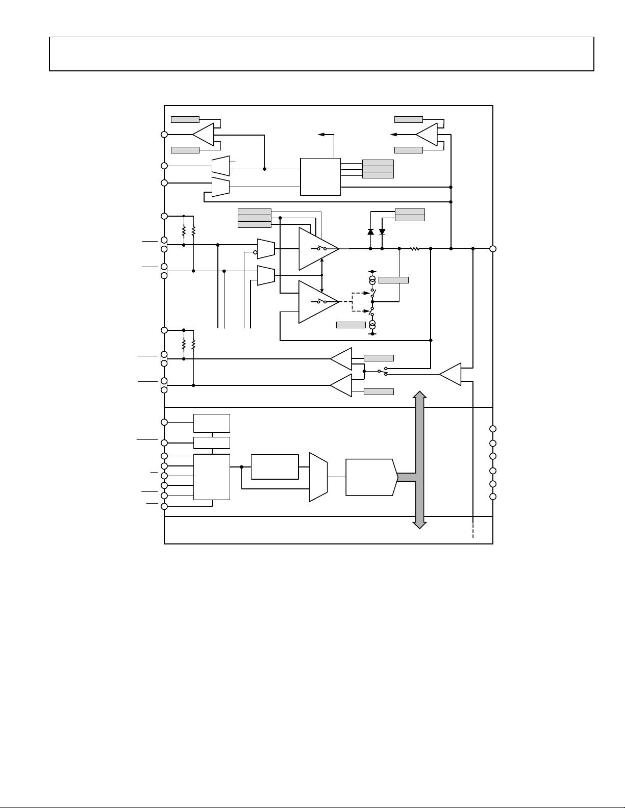
GENERAL DESCRIPTION
The ADATE320 is a complete, single-chip ATE solution that
performs the pin electronics functions of a driver, comparator,
and active load (DCL), and a four quadrant per pin parametric
measurement unit (PPMU). Dedicated 16-bit digital-to-analog
converters (DACs) with on-chip calibration registers provide all
the necessary dc levels for operation of the device.
The driver features three active modes: high, low, and terminate, as
well as a high impedance inhibit state. The inhibit state, in
conjunction with the integrated dynamic clamps, facilitates
significant attenuation of transmission line reflections when the
driver is not actively terminating the line. The open-circuit drive
capability is −1.5 V to +4.5 V to accommodate a standard range
of ATE and instrumentation applications.
The ADATE320 can be used as a dual, single-ended pin
electronics channel or as a single differential channel. In
addition to per channel high speed window comparators, the
ADATE320 provides a programmable threshold differential
comparator for differential ATE applications.
All dc levels for DCL and PPMU functions are generated by
dedicated, on-chip, 16-bit DACs. To facilitate the programming
of accurate levels, the ADATE320 includes an integrated
calibration function to correct for the gain and offset errors of
each functional block. Correction coefficients can be stored on
chip, and any values written to the DACs adjust automatically
using the appropriate correction factors.
The A
DATE320 uses a serial programmable interface (SPI) bus
to program all functional blocks, DACs, and on-chip calibration
constants. It also has an on-chip temperature sensor and overvolt-
age/undervoltage fault clamps that monitor and report the
device temperature and any output pin or transient PPMU
voltage faults that may occur during operation.
The ADATE320 is available in two options. The standard option
has high speed comparator outputs with 250 mV output swing.
The ADATE320-1 has 400 mV output swing. See the Ordering
Guide for more information.
ADATE320* PRODUCT PAGE QUICK LINKS
Last Content Update: 02/23/2017
COMPARABLE PARTS
View a parametric search of comparable parts.
DOCUMENTATION
Data Sheet
• ADATE320: 1.25 GHz Dual Integrated DCL with PPMU,
Level Setting DACs, and On-Chip Calibration Registers
Data Sheet
DESIGN RESOURCES
• ADATE320 Material Declaration
• PCN-PDN Information
• Quality And Reliability
• Symbols and Footprints
DISCUSSIONS
View all ADATE320 EngineerZone Discussions.
SAMPLE AND BUY
Visit the product page to see pricing options.
TECHNICAL SUPPORT
Submit a technical question or find your regional support
number.
DOCUMENT FEEDBACK
Submit feedback for this data sheet.
This page is dynamically generated by Analog Devices, Inc., and inserted into this data sheet. A dynamic change to the content on this page will not
trigger a change to either the revision number or the content of the product data sheet. This dynamic page may be frequently modified.
ADATE320 Data Sheet
Rev. B | Page 2 of 82
TABLE OF CONTENTS
Features .............................................................................................. 1
Applications ....................................................................................... 1
General Description ......................................................................... 1
Revision History ............................................................................... 2
Functional Block Diagram .............................................................. 3
Specifications ..................................................................................... 4
Electrical Specifications ............................................................... 4
Driver Specifications .................................................................... 5
Reflection Clamp Specifications ................................................. 7
Normal Window Comparator (NWC) Specifications ............. 8
Differential Mode Comparator (DMC) Specifications ......... 10
Active Load Specifications ........................................................ 11
PPMU Specifications ................................................................. 13
PPMU Go/No-Go Comparators Specifications ..................... 18
PPMU External Sense Pins Specifications .............................. 18
VREF, VREFGND, and DUTGND Reference Input Pins
Specifications .............................................................................. 19
Temperature Monitor Specifications ....................................... 19
Alarm Functions Specifications................................................ 19
Serial Programmable Interface (SPI) Specifications .............. 20
SPI Timing Specifications ......................................................... 20
SPI Timing Diagrams ................................................................. 21
Absolute Maximum Ratings .......................................................... 25
Thermal Characteristics ............................................................ 25
Explanation of Test Levels ......................................................... 25
ESD Caution................................................................................ 25
User Information and Truth Tables ......................................... 26
Pin Configuration and Function Descriptions ........................... 28
Typical Performance Characteristics ........................................... 30
Theory of Operation ...................................................................... 50
Serial Programmable Interface (SPI) ....................................... 50
Level Setting DACs .................................................................... 52
Alarm Functions ......................................................................... 59
Applications Information .............................................................. 62
Power Supply, Grounding, and Typical Decoupling Strategy
....................................................................................................... 62
Power Supply Sequencing ......................................................... 64
Detailed Functional Block Diagrams ........................................... 65
SPI Register Memory Map and Details ....................................... 71
Memory Map .............................................................................. 71
Register Details ........................................................................... 74
Default Test Conditions ................................................................. 80
External Components .................................................................... 81
Outline Dimensions ....................................................................... 82
Ordering Guide .......................................................................... 82
REVISION HISTORY
9/2016—Rev. A to Rev. B
Changes to Time Constant 1 Parameter and Time Constant 2
Parameter, Table 2 ............................................................................. 7
Changes to IOx Offset Parameter, and IOHx Offset
Parameter, Table 6 ........................................................................... 11
Change to AGND Pin Number Column ..................................... 29
Change to SPI Reset Sequence and the
RST
Pin Section .......... 50
Changes to the SPI Clock Cycles and
BUSY
Pin Section .......... 51
Changes to Table 24 ........................................................................ 54
Changes to Figure 137 .................................................................... 65
10/2015—Revision A: Initial Version
Data Sheet ADATE320
Rev. B | Page 3 of 82
FUNCTIONAL BLOCK DIAGRAM
+
–
VIL0
VIT0/VCOM0
VIH0
VOL0
DUT0
VTTD0
CMPH0/CMPH0
CMPL0/CMPL0
NWC
NWC
DIFF
DRIVER
LOAD
COMPARATOR
50Ω
PPMU_S0
THERM
PPMU_M0
PMU
CHANNEL 0
S
F
OUT
PMU0
PCH0
PCL0
VCH0
VCL0
OVDH
OVDL
TO ALARM
(HIGH/LOW
VOLTAGE FAULT)
PPMU_CMP0
VTTC0
DAT1
RCV1
(FROM CHANNEL 1)
TO ALARM
(HIGH/LOW
CLAMP FAULT)
POH0
POL0
MUX
OVER
VOLTAGE
MUX
MUX
MUX
CHANNEL 1
(SAME AS CHANNEL 0 EXCEPT WHERE NOTED ABOVE)
COMMON
SPI
RST
MUX
TEMP
SENSOR
VTHERM
ALARM
ALARM
VDD
AGND
PGND
VEE
DGND
(FROM DUT)
DAT0
RCV0
(TO CHANNEL 1)
VCC
SDO
SCLK
SDI
DAT0/DAT0
RCV0/RCV0
GAIN/OFFSET
CORRECTION
2 × 16
16-BIT DACs
BUSY
CS
CH0 ONLY
IOH0
IOL0
PPMU
GO/NO-GO
50Ω
50Ω
VOH0
12160-001
Figure 1.
ADATE320 Data Sheet
Rev. B | Page 4 of 82
SPECIFICATIONS
V
CC
= 8.0 V, V
DD
= 1.8 V, V
EE
= −5.0 V, V
TTCx
= V
TTDx
= 1.2 V, V
REF
= 2.500 V, V
REFGND
= 0.000 V. All default test conditions are as defined in
Table 30. All specified values are at T
J
= 60°C, where T
J
corresponds to the typical internal temperature sensor reading (VTHERM pin), unless
otherwise noted. Temperature coefficients are measured around T
J
= 40°C, 60°C, 80°C, and 100°C. Typical values are based on the
statistical mean of the design, simulation analyses, and/or limited bench evaluation data. Typical values are neither tested nor guaranteed.
Test level codes are defined in the Explanation of Test Levels section.
ELECTRICAL SPECIFICATIONS
Table 1.
Parameter Min Typ Max Unit Test Level Test Conditions/Comments
DUTx PIN CHARACTERISTICS
Output Leakage Current
DCL Disable
PPMU Range E −10.0 +5.0 +10.0 nA P −1.5 V < V
DUTx
< +4.5 V, PPMU and DCL disabled, PPMU
Range E, VCLx = −2.5 V, VCHx = +7.5 V
PPMU Range A to
Range D
5.0 nA C
T
−1.5 V < V
DUTx
< +4.5 V, PPMU and DCL disabled, PPMU Range A,
Range B, Range C, and Range D, VCLx = −2.5 V, VCHx = +7.5 V
Driver High-Z Mode −0.4 +0.4 µA P −1.5 V < V
DUTx
< +4.5 V, PPMU disabled and DCL enabled,
RCV active, VCLx = −2.5 V, VCHx = +7.5 V
Capacitance 0.4 pF S Drive VITx = 0.0 V
Voltage Range
−1.5
+4.5
V
D
POWER SUPPLIES Power measured with the DUTx pin high-Z, 10 K to 0.0 V
Positive DCL Supply, V
CC
7.6 8.0 8.4 V D Defines dc power supply rejection (PSR) conditions
Negative DCL Supply, V
EE
−5.25 −5.0 −4.75 V D Defines dc PSR conditions
Digital Supply, V
DD
1.7 1.8 1.9 V D
Comparator Termination,
V
TTCx
0.5 1.2 1.8 V D VTTC0 is not electrically connected to VTTC1
Driver Termination, V
TTDx
0.0 1.2 1.8 V D VTTD0 is not electrically connected to VTTD1
Positive DCL Supply
Current, I
CC
Load and PPMU power-down
ADATE320 145 169 185 mA P
ADATE320-1 145 169 185 mA P
Negative DCL Supply
Current, I
EE
Load and PPMU power-down
ADATE320
190
222
235
mA
P
ADATE320-1 220 247 265 mA P
Digital Core Supply
Current, I
DD
−125 +10 +125 μA P Quiescent (SPI is static)
Comparator Termination
Supply Current, V
TTCx
0.5 V ≤ V
TTCx
≤ 1.8 V
ADATE320
41
mA
C
T
ADATE320-1 66 mA C
T
Driver Termination Supply
Current, V
TTDx
0 mA C
T
0.0 V ≤ V
TTDx
≤ 1.8 V, (DATx +
DATx
)/2 = (RCVx +
RCVx
)/2 = V
TTDx
Total Power Dissipation Load and PPMU power-down
ADATE320 2.10 2.52 2.75 W P
ADATE320-1
2.25
2.66
2.90
W
P
剩余82页未读,继续阅读
资源评论
凤海芯盛
- 粉丝: 90
- 资源: 13
上传资源 快速赚钱
- 我的内容管理 展开
- 我的资源 快来上传第一个资源
- 我的收益 登录查看自己的收益
- 我的积分 登录查看自己的积分
- 我的C币 登录后查看C币余额
- 我的收藏
- 我的下载
- 下载帮助
安全验证
文档复制为VIP权益,开通VIP直接复制
信息提交成功